Get Latest Exam Updates, Free Study materials and Tips

1. Which of the following condition is true for cut-off mode?
a) The collector current Is zero
b) The collector current is proportional to the base current
c) The base current is non zero
d) All of the mentioned
Answer: a
Explanation: The base current as well as the collector current are zero in cut-off mode.
2. Which of the following is true for the cut-off region in an npn transistor?
a) Potential difference between the emitter and the base is smaller than 0.5V
b) Potential difference between the emitter and the base is smaller than 0.4V
c) The collector current increases with the increase in the base current
d) The collector current is always zero and the base current is always non zero
Answer: b
Explanation: Both collector and emitter current are zero in cut-off region.
3. Which of the following is true for a typical active region of an npn transistor?
a) The potential difference between the emitter and the collector is less than 0.5 V
b) The potential difference between the emitter and the collector is less than 0.4 V
c) The potential difference between the emitter and the collector is less than 0.3 V
d) The potential difference between the emitter and the collector is less than 0.2 V
Answer: c
Explanation: Most commonly used transistors have Vce less than 0.4 V for the active region.
4. Which of the following is true for the active region of an npn transistor?
a) The collector current is directly proportional to the base current
b) The potential difference between the emitter and the collector is less than 0.4 V
c) All of the mentioned
d) None of the mentioned
Answer: c
Explanation: The base current and the collector current are directly proportional to each other and the potential difference between the collector and the base is always less than 0.4 V.
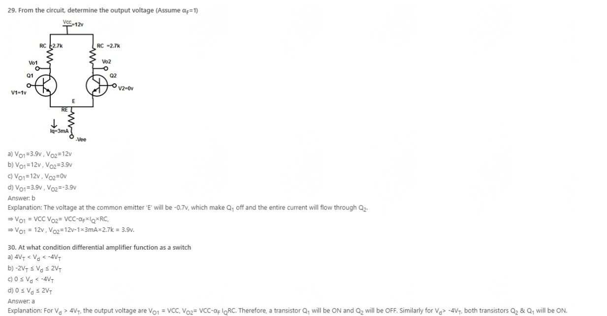
5. Which of the following is true for the saturation region of BJT transistor?
a) The collector current is inversely proportional to the base current
b) The collector current is proportional to the square root of the collector current
c) The natural logarithm of the collector current is directly proportional to the base current
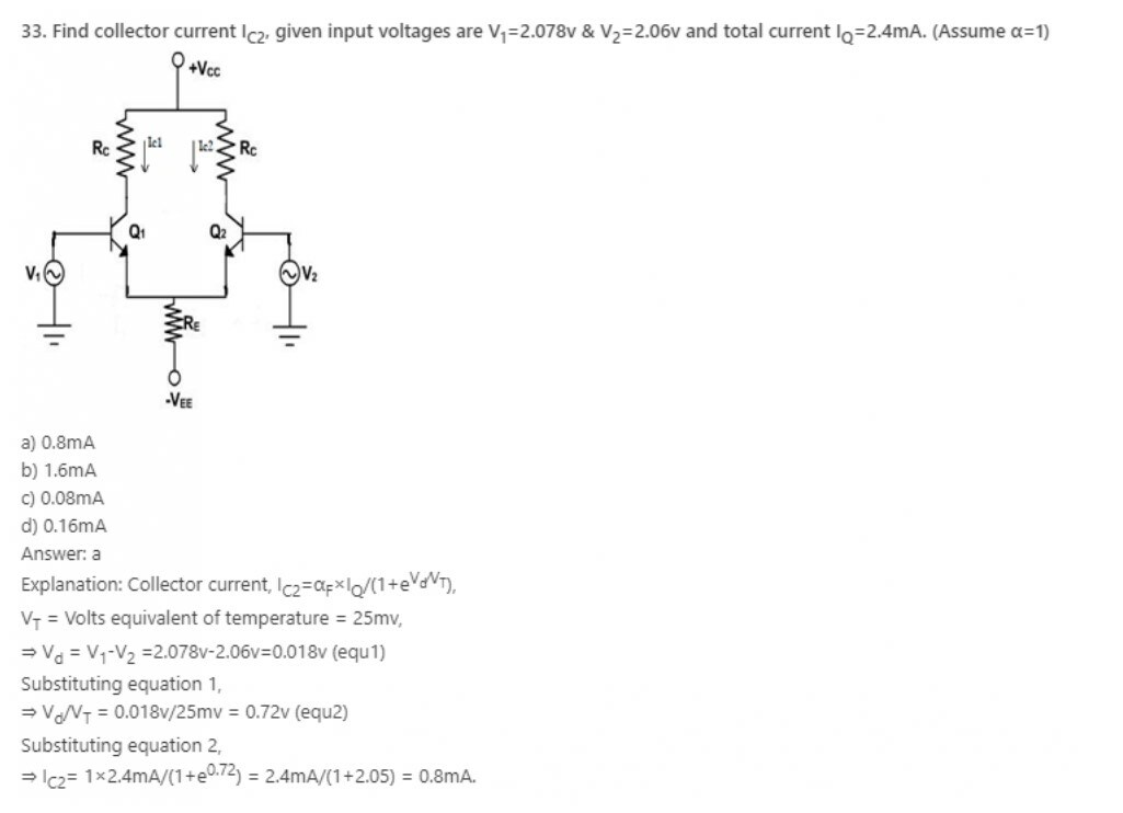
d) None of the mentioned
Answer: b
Explanation: The collector current is directly proportional to the base current in the saturation region of the BJT.
6. Which of the following is true for a npn transistor in the saturation region?
a) The potential difference between the collector and the base is approximately 0.2V
b) The potential difference between the collector and the base is approximately 0.3V
c) The potential difference between the collector and the base is approximately 0.4V
d) The potential difference between the collector and the base is approximately 0.5V
Answer: d
Explanation: The commonly used npn transistors have a potential difference of around 0.5V between he collector and the base.
7. The potential difference between the base and the collector Vcb in a pnp transistor in saturation region is ________
a) -0.2 V
b) -0.5V
c) 0.2 V
d) 0.5 V
Answer: b
Explanation: The value of Vcb is -0.5V for a pnp transistor and 0.5V for an npn transistor.
8. For a pnp transistor in the active region the value of Vce (potential difference between the collector and the base) is
a) Less than 0.3V
b) Less than 3V
c) Greater than 0.3V
d) Greater than 3V
Answer: a
Explanation: For a pnp transistor Vce is less than 0.3V, for an npn transistor it is greater than 0.3V.
9. Which of the following is true for a pnp transistor in active region?
a) CB junction is reversed bias and the EB junction is forward bias
b) CB junction is forward bias and the EB junction is forward bias
c) CB junction is forward bias and the EB junction is reverse bias
d) CB junction is reversed bias and the EB junction is reverse bias
Answer: a
Explanation: Whether the transistor in npn or pnp, for it be in active region the EB junction must be reversed bias the CB junction must be forward bias.
10. Which of the following is true for a pnp transistor in saturation region?
a) CB junction is reversed bias and the EB junction is forward bias
b) CB junction is forward bias and the EB junction is forward bias
c) CB junction is forward bias and the EB junction is reverse bias
d) CB junction is reversed bias and the EB junction is reverse bias
Answer: b
Explanation: Whether the transistor in npn or pnp, for it be in saturation region the EB junction must be forward bias the CB junction must be forward bias.
11. BJT is biased to _________
a) Work as a switch
b) Prevent thermal runaway
c) Increase DC collector current
d) Operate it in the saturation region
Answer: b
Explanation: A BJT is biased to operate in the active region, to work as an amplifier. It is not biased in the cut-off or saturation region to work as a switch. Also, biasing is done to maintain a stable collector current so that the operating point does not change. This also prevents thermal runaway.
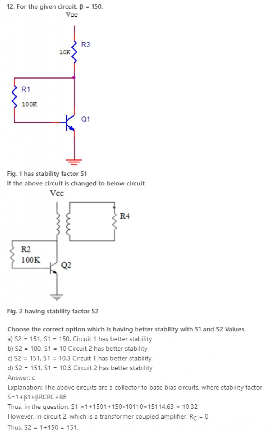
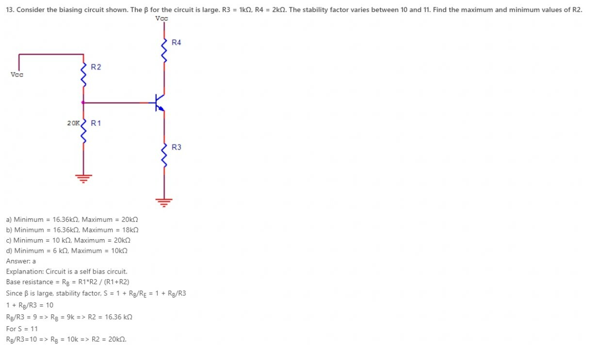
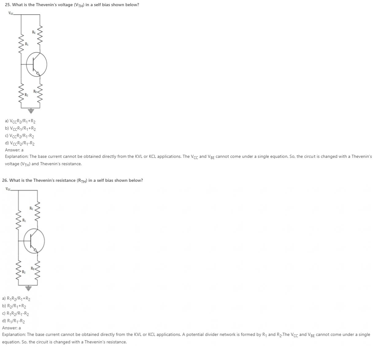
14. Choose the incorrect option according to self bias circuit?
a) Voltage gain increases
b) Stability factor is independent of collector resistance
c) BJT can be used in either of the three configurations
d) Excellent stability in collector current is achieved
Answer: d
Explanation: In a self bias circuit, due to emitter resistance a negative feedback exists. This decreases voltage gain. Also, stability factor S does not depend on collector resistance, only on base and emitter resistance and β, if required. S=(1+β)(RB+RE)RB+(1+β)RE.
S is least in self bias circuit, hence excellent stability is achieved.
17. Why is self bias circuit not used in IC amplifier?
a) To reduce power losses
b) To reduce area used on the chip
c) Stability factor reduces in the IC
d) Voltage gain is reduced
Answer: b
Explanation: Self biased circuits are not preferred in IC amplifiers because they need large resistances R1 and R2, since then S will be smaller and stability will be more. However, using large resistances in ICs means a requirement of larger chip area, so to reduce this area requirement, we use current mirror circuits instead.
20. Widlar current source was introduced to obtain a smaller output current.
a) True
b) False
Answer: a
Explanation: In a current mirror circuit, to obtain lower values of output current, the resistance values required to increase a lot, which becomes difficult to manufacture on an IC. Instead, we use a widlar current source, where an emitter resistance is also present, affecting the output current.
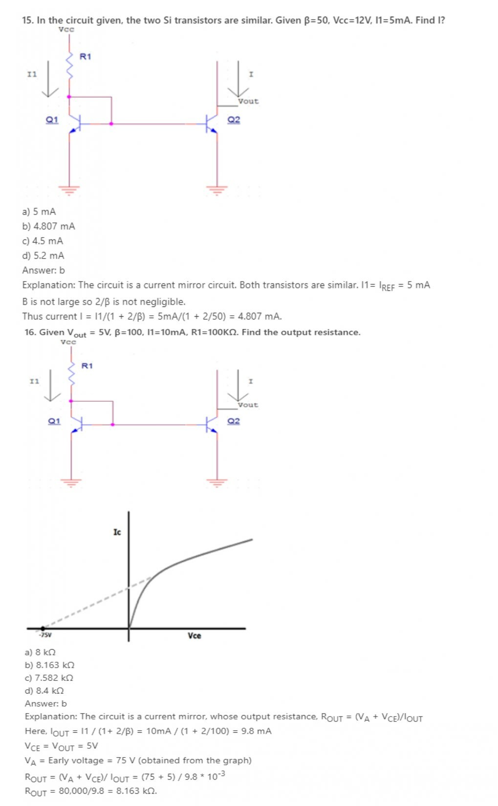
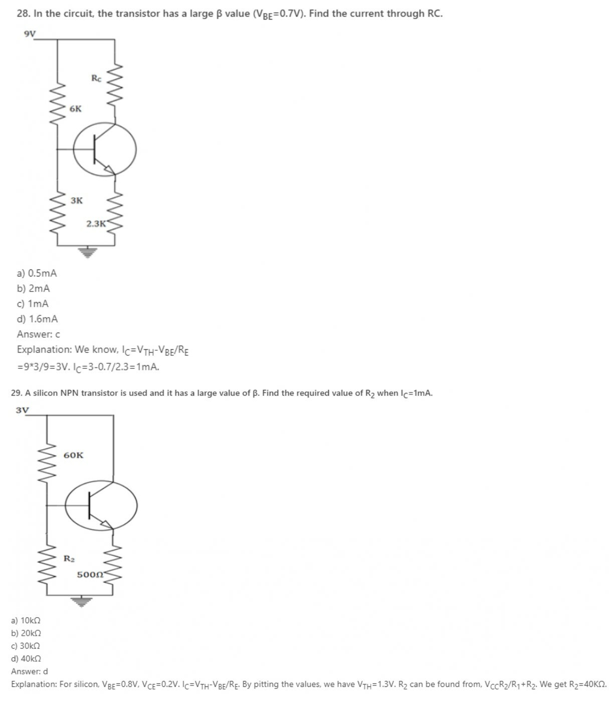
21. The collector current (IC) that is obtained in a self biased transistor is_________
a) (VTH – VBE)/RE
b) (VTH + VBE)/RE
c) (VTH – VBE)/RE
d) (VTH + VBE)/RE
Answer: a
Explanation: The collector current is analysed by the DC analysis of a transistor. It involves the DC equivalent circuit of a transistor. The base current is first found and the collector current is obtained from the relation, IC=IBβ.
22. The collector to emitter voltage (VCE) is obtained by_________
a) VCC – RCIC+RBIB
b) VCC – RCIC-REIE
c) VCC + RCIC
d) VCC + RCIB
Answer: b
Explanation: The collector to emitter voltage is obtained in order to find the operating point of a transistor. It is taken when there is no signal applied to the transistor. The point thus obtained lies in the cut off region when the transistor is used as a switch.
23. The thermal runway is avoided in a self bias because_________
a) of its independence of β
b) of the positive feedback produced by the emitter resistor
c) of the negative feedback produced by the emitter resistor
d) of its dependence of β
Answer: c
Explanation: The self destruction of a transistor due to increase temperature is called thermal run away. It is avoided by the negative feedback produced by the emitter resistor in a self bias. The IC which is responsible for the damage is reduced by decreased output signal.
24. When the temperature is increased, what happens to the collector current after a feedback is given?
a) it remains same
b) it increases
c) it cannot be predicted
d) it decreases
Answer: d
Explanation: Before the feedback is applied, when the temperature is increased, the reverse saturation increases. The collector current also increases. When the feedback is applied, the drop across the emitter resistor increases with decreasing collector current and the thermal runway too.
27. The stability factor for a self biased transistor is_________
a) 1 – RTH/RE
b) 1 + RTH/RE
c) 1 + RE/RTH
d) 1 – RE/RTH
Answer: b
Explanation: The stability of the circuit is inversely proportional to the stability factor. The emitter resistor is very large when compared to the Thevenin’s resistance. When β is not that large, then S=(1+ β)( RTH+ RE)/ (1+ β)RE+ RTH.
30. The value of αac for all practical purposes, for commercial transistors range from_________
a) 0.5 to 0.6
b) 0.7 to 0.77
c) 0.8 to 0.88
d) 0.9 to 0.99
Answer: d
Explanation: For all practical purposes, αac=αdc=α and practical values in commercial transistors range from 0.9-0.99. It is the measure of the quality of a transistor. Higher is the value of α, better is the transistor in the sense that collector current approaches the emitter current.
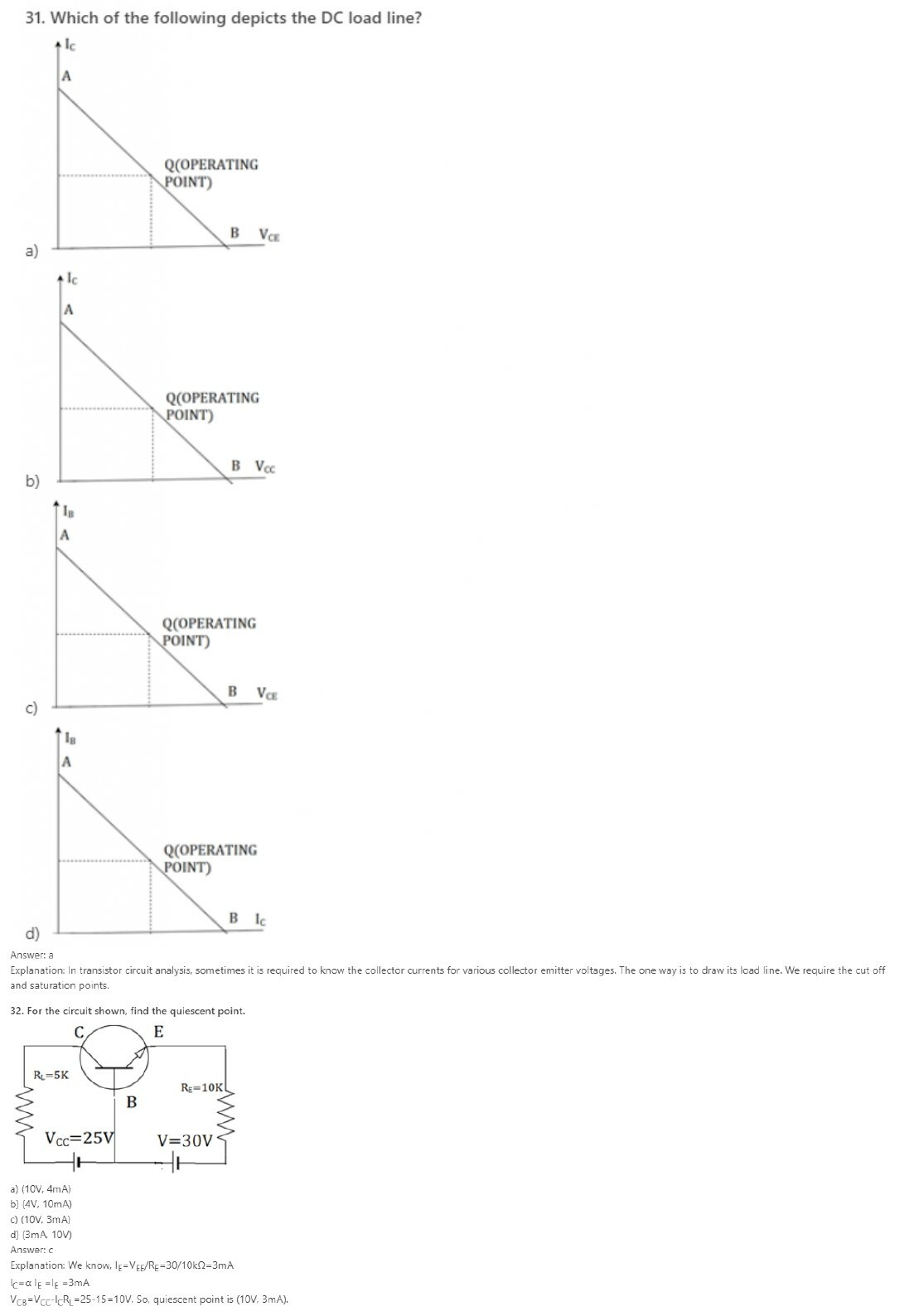
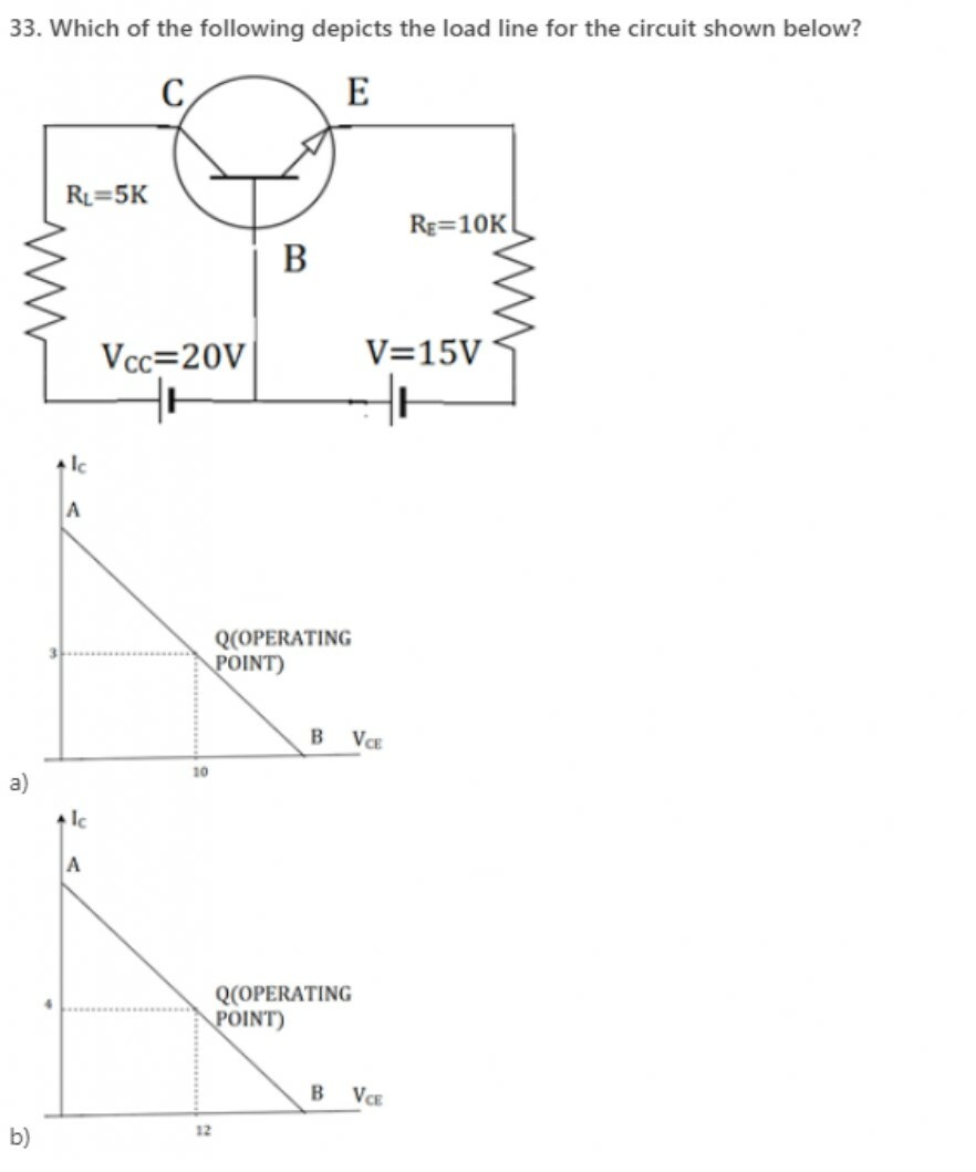
39. What is the DC characteristic used to prove that the transistor is indeed biased in saturation mode?
a) IC = βIB
b) IC > βIB
c) IC >> βIB
d) IC < βIB
Answer: d
Explanation: When in a transistor is driven into saturation, we use VCE(SAT) as another linear parameter. In, addition when a transistor is biased in saturation mode, we have IC < βIB. This characteristic used to prove that the transistor is indeed biased in saturation mode.
41. Which type of amplifiers exhibits the current gain approximately equal to unity without any current amplification?
a) CE
b) CB
c) CC
d) Cascade
Answer: b
Explanation: In common base amplifier, input signal is applied at emitter terminal while the amplified output signal is obtained at the collector terminal with respect to ground.
For the AC signals, the base terminal is specifically connected to ground through the capacitor.
Even, the output resistance is very high & hence, the current gain is approximately equal to unity. Due to this, there is no possibility of current amplification. Consequently, the CB amplifier exhibits high voltage gain.
42. Why is the Darlington configuration not suitable for more than two transistors?
a) Because leakage current increases and voltage gain decreases with multiple numbers of transistors
b) Because leakage current decreases and voltage gain increases with multiple numbers of transistors
c) Because leakage current as well as voltage gain increases with multiple numbers of transistors
d) Because leakage current as well as voltage gain decreases with multiple numbers of transistors
Answer: a
Explanation: As the number of transistors increases, the leakage current also increases. The leakage current gets multiplied by the current gain of Darlington configuration.
Generally, the voltage gain of CC configuration is nearly equal to ‘1’ but the voltage gain of Darlington configuration is very less than ‘1’.
Therefore, if we increase the number of transistors in Darlington configuration the voltage gain will ultimately reduce. But, in order to prevent these likely undesirable conditions, Darlington configuration is completely inappropriate for more than two transistors.
43. What should be the level of input resistance to allow the occurrence of source loading in common base amplifier configuration?
a) low
b) high
c) moderate
d) stale
Answer: a
Explanation: As per the configuration of CB amplifier, it is evident that its input resistance is very low but its output resistance is enormously high.
However, the lower value of input resistance allows the stipulation of source loading in common base amplifier circuit.
Thus, there is no current amplification because of unity current gain. These all reasons eventually add to high level of voltage gain.
44. Which among the below assertions is not a relevant property of CE amplifier?
a) High voltage gain
b) High current gain
c) High input resistance
d) High output resistance
Answer: d
Explanation: The voltage gain, current gain and input resistance CE amplifiers are utterly high but it has low output resistance.
The collector resistor (Rc) performs the purpose of controlling the collector current. Input and emitter resistors are adopted for biasing of transistor in an active region so that it becomes possible for the transistor to function as an amplifier.
Due to high current gain at the output of RC coupled CE amplifier, the resistance level at the output is exceedingly low.
45. What is the phase-shift between input and output voltages of CE amplifier?
a) 90°
b) 120°
c) 180°
d) 270°
Answer: c
Explanation: During the amplification method of RC coupled CE amplifier, there is a phase shift of about 180o between input and output. Basically, the output is said to be reversed version of input.
The magnitude of output voltage becomes higher as compared to that of input signal but the shape is correctly similar to that of an input signal.
But, the input ac signal gets amplified along with the phase-shift of 180o between input and output.
46. Which capacitor is used to block DC portion by allowing to pass only AC portion of the amplified signal to load?
a) Input Coupling Capacitor
b) Bypass Capacitor
c) Output Coupling Capacitor
d) Both coupling and bypass capacitor
Answer: c
Explanation: In RC coupled CE amplifier, the transistor is connected in common-emitter (CE) configuration and capacitors C1 & C2 are coupling capacitors.
Input coupling capacitor is used for coupling the ac input voltage to the transistor base. Inversely, the output coupling capacitor (C2) is used for coupling an output of an amplifier to the load resistance or to the next stage of an amplifier.
Besides these, input coupling capacitor blocks any DC element present in AC input voltage & couples only AC component of input signal whereas bypass capacitor offers a low reactance to the amplified AC signal.
47. The configuration in which voltage gain of transistor amplifier is lowest is ____________
a) common collector
b) common emitter
c) common base
d) common emitter & base
Answer: a
Explanation: In common collector configuration (also known as the emitter follower) because the emitter voltage follows that of the base. Offering a high input impedance and a low output impedance it is extensively used as a buffer. The voltage gain is unity, even though current gain is high. The input and output signals are in phase.
48. The configuration in which current gain of transistor amplifier is lowest is ___________
a) common collector
b) common base
c) common emitter
d) common emitter & base
Answer: b
Explanation: In Common base configuration, the input impedance is very low; While offering a high output impedance. Although the voltage is high, the current gain is low and the overall power gain is also low when compared to the other transistor configurations available. Thus, there is no current amplification because of unity current gain.
49. The configuration in which input impedance of transistor amplifier is lowest is ___________
a) common collector
b) common emitter
c) common base
d) common emitter & base
Answer: c
Explanation: In Common base configuration, the input impedance is very low; While offering a high output impedance. Although the voltage is high, the current gain is low and the overall power gain is also low when compared to the other transistor configurations available.
50. The configuration in which output impedance of transistor amplifier is highest is ___________
a) common collector
b) common base
c) common emitter
d) common collector and base
Answer: b
Explanation: In Common base configuration, the input impedance is very low; While offering a high output impedance. Although the voltage is high, the current gain is low and the overall power gain is also low when compared to the other transistor configurations available.
51. Q. What should be the gain of an amplifier at 20 kHz if the half power frequencies are fL = 20 Hz and fH = 15 kHz along with mid band gain = 80?
a) 22.76
b) 45.09
c) 40.08
d) 48.07
Answer: d
Explanation:
fL = 20 Hz
fH = 15 kHz
Av(mid) = 80
To determine: Voltage gain at 20 kHz
Formula : Av = Av(mid) / √1 + (f/fH)2
To determine the voltage gain at 20 kHz, we recognize that,
Av = Av(mid) / √1 + (f/fH)2
= 80 / √1 + (20 k/15k)2
= 48.07.
52. Which of the following is true?
a) Ib = ß Ic
b) Ib = ß + 1/ Ic
c) Ib = Ic/ß
d) Ib = Ic/ ß – 1
Answer: c
Explanation: The correct relationship between Ic and Ie is Ib = Ic/ß.
53. The SI units of transconductance is
a) Ampere/ volt
b) Volt/ ampere
c) Ohm
d) Siemens
Answer: a
Explanation: Transcoductance is given by Ic/Vt.
54. Which of the following represents the correct mathematical form of the term denoted by the symbol Rp?
a) ß/gm
b) Vt/Ib
c) All of the mentioned
d) None of the mentioned
Answer: c
Explanation: Both of the expressions are identical.
1. The use of amplifier in a circuit is to _____________ for input signal.
a) Provide a phase shift
b) Provide strength
c) Provide frequency enhancement
d) Make circuit compatible
Answer: b
Explanation: The only use of amplifier in a circuit is to provide strength to signal. This may refer to an increase in current, voltage or power of the output w.r.t the input being applied.
2. The unwanted characteristics of amplifier output apart from the desired output is collectively termed as ___________
a) Inefficiency
b) Damage
c) Fault
d) Distortion
Answer: d
Explanation: The unwanted characteristics of amplifier output apart from desired output is collectively termed as distortion. This should be avoided.
3. Unit of power rating of a transistor is expressed in ___________
a) Watts
b) KWh
c) W/s
d) Wh
Answer: a
Explanation: Power rating is the maximum power allowable to dissipate by a transistor beyond this point transistor may behave unlikely. This is expressed in watts.
4. Which device was used for the amplification of audio signals before the invention of power amplifiers?
a) Diode
b) Op-amp
c) Vacuum tubes
d) SCR
Answer: c
Explanation: Before the invention of power amplifier vacuum tubes are used for audio signal amplification which consumes large space and costly.
5. Power amplifier directly amplifies ___________
a) Voltage of signal
b) Current of the signal
c) Power of the signal
d) All of the mentioned
Answer: d
Explanation: Power amplifier increases voltage as well as current. Increase in voltage or current is small compared to normal amplifiers. But power amplification has occurred ie. Voltage x current is more.
6. Input stage of power amplifier is also called ___________
a) First op
b) Beginning stage
c) Front end
d) Normal stage
Answer: c
Explanation: Input stage of the power amplifier is also called the front end.
7. Transistor in power amplifier is ___________
a) An active device
b) A passive device
c) A op-amp
d) A voltage generating device
Answer: a
Explanation: Transistor is an active device since transistor contains voltage sources which are necessary for amplification.
8. For a perfect power amplifier output power rating will be ________ if the output impedance is halved.
a) Halved
b) Squared
c) Doubled
d) Square rooted
Answer: c
Explanation: In the equation of power output for the power amplifier, the power is proportional to the square of the current and inversely proportional to the resistance. If the impedance is halved then power is doubled.
9. Which of the following audio speaker will be hard to be driven by a power amplifier?
a) 4ohm
b) 8ohm
c) 12ohm
d) 2ohm
Answer: d
Explanation: If the resistance of the audio amplifier is less, the output power of the transistor will be high since output current is increasing. Hence to drive 2ohm speaker amplifier needs double power that for 4ohm speaker.
10. The power rating of the amplifier is 100watts then the transistor can only operate at ___________
a) Power higher than 100w
b) Power lower than 100w
c) Power near to 100w
d) Power lower than 200W
Answer: b
Explanation: The power rating is 100 W, and that is the maximum allowable power usage of a transistor, beyond which it may damage. If the power is less than 100W, the circuit operates. Near to 100W, the power may also be higher than 100W, hence that option is incorrect.
11. Which of the following amplifier class have highest linearity and lowest distortion?
a) Class A
b) Class B
c) Class C
d) Class B push-pull
Answer: a
Explanation: Class A amplifier has the highest linearity and the lowest distortion. The amplifying element is always conducting and close to the linear portion of its transconductance curve. The point where the device is almost off is not at a zero signal point and hence its distortions compared to other classes are less.
12. Which of the following letter is not used to represent a class?
a) D
b) E
c) C
d) K
Answer: d
Explanation: There is no amplifier called Class K. There are only A, B, C, D,E/F, G, H, S.
13. Which of the following letter is not used to represent a class?
a) I
b) H
c) G
d) S
Answer: a
Explanation: There is no amplifier called Class I. There are only A, B, C, D, E/F, G, H, S.
14. Which of the following class has poorest linearity
a) Class A
b) Class B
c) Class C
d) Class AB
Answer: c
Explanation: Class C amplifiers have high efficiency but have the poorest linearity since they only take less than 180° oscillations. They are suitable for amplifying constant envelope signals.
15. Which of the following amplifier cannot be used for audio frequency amplification?
a) Class A
b) Class C
c) Class AB
d) Class B push-pull
Answer: b
Explanation: Class C amplifier cannot be used for audio frequency amplifiers because of its high distortion.
16. Which of the following amplifier is less efficient than others?
a) Class C
b) Class B
c) Class A
d) Class AB
Answer: c
Explanation: Class A amplifiers are the least efficient of all. A maximum of 25% theoretical efficiency is obtainable, 50% for when using transformer or with induced coupling. This wastes power, as well as increases the cost and requires higher rated output devices.
17. Which of the following amplifier is designed to operate in digital pulses?
a) Class D
b) Class C
c) Class AB
d) Class B
Answer: a
Explanation: Class D amplifiers use a form of PWM to control the output devices. Conduction angle varies with the pulse width and doesn’t depend on the input directly. The analog signal is converted into a stream of pulses representing the signal using a modulation technique.
18. Which of the following class have a theoretical efficiency of 50%?
a) Class A
b) Class C
c) Class AB
d) Class D
Answer: a
Explanation: Class A amplifier has a theoretical efficiency of 50%. 50% of the energy supplied is a waste.
19. Which of the following class have a theoretical efficiency of 78.5%?
a) Class A
b) Class D
c) Class C
d) Class B
Answer: d
Explanation: Class B amplifier has a theoretical efficiency of 78.5% which higher than Class A while Class D theoretically have efficiency of 100%.
20. Which of the following amplifier is most suited for making tuning circuits?
a) Class A
b) Class B
c) Class C
d) Class D
Answer: c
Explanation: Class C is most suitable amplifier type for tuning circuit and radio frequency amplification. It employs filtering and hence the final signal is completely acceptable. Class C amplifiers are quite efficient than other types.
21. Oscillators are used to ______ AC voltage.
a) Prevent
b) Generate
c) Amplify
d) Rectify
Answer: b
Explanation: Oscillators are used for generating AC voltage. They are often characterized by the frequency of the oscillations produced. There are two main types of electronic oscillators, linear/harmonic and nonlinear/relaxation oscillator.
22. Oscillator __________ an AC input for giving an AC output.
a) Doesn’t need
b) Need
c) Doesn’t need at lower frequencies
d) Doesn’t need at higher frequencies
Answer: a
Explanation: An oscillator is an amplifier with positive feedback. It usually has a noise which is amplifier as an oscillating output. They do not require any type of specific input to function properly.
23. Negative resistance are incorporated in oscillator for ___________
a) Sustained oscillation
b) Damped oscillation
c) Biasing the oscillator
d) Increasing amplitude of oscillation
Answer: a
Explanation: Negative resistance are incorporated in oscillator for sustained oscillation. Negative resistance will cancel the damping by positive (normal) resistance.
24. For accomplishing negative resistance in oscillator we use _____________
a) Voltage divider circuit
b) Negative feedback
c) Positive feedback
d) Current divider circuit
Answer: c
Explanation: The input or output impedance of an amplifier with positive feedback applied, can be negative. When loop gain is greater than 1, the input impedance is a negative value, over a linear range. These are also called active resistors.
25. Primary trigger for oscillation is obtained from ___________
a) DC voltage
b) Noise voltage
c) External trigger voltage
d) No trigger is required
Answer: b
Explanation: The primary trigger for oscillation is obtained from noise voltage.
26. The AC power of output signal is obtained by ___________
a) Input AC voltage
b) Input DC voltage
c) DC biasing voltage
d) Power is generated by transistor itself
Answer: c
Explanation: The Ac power of output signal is obtained by DC biasing voltage of amplifier.
27. The output of a stable oscillator have ___________
a) Constant amplitude
b) Varying amplitude
c) Constant amplitude at high frequencies only
d) Constant amplitude at low frequencies only
Answer: a
Explanation: Output of a stable oscillator have constant amplitude and frequency. A common criteria is the Barkhausen stability criteria, wherein it states that loop gain should be unity and feedback should be positive.
28. The output waveform of a stable oscillator have ___________
a) Constant frequency at low amplitude only
b) Constant frequency at high amplitude only
c) Variable frequency
d) Constant frequency
Answer: d
Explanation: Output of a stable oscillator have constant amplitude and frequency.
29. In an oscillator if phase of feedback is same as that of oscillation waveform then feedback is called ___________
a) Positive feedback
b) Negative feedback
c) Cannot be predicted
d) Either positive or negative depending upon frequency
Answer: a
Explanation: In an oscillator if phase of feedback is same as that of oscillation waveform then feedback is called positive feedback.
30. The output of oscillator will not depend upon ___________
a) Feedback
b) Amplifier
c) Both feedback and amplifier
d) Input voltage
Answer: d
Explanation: The output of oscillator will not depend upon input voltage. There is no input voltage for an oscillator.
31. Which of the following is not an example for non-sinusoidal oscillator?
a) Sawtooth Generators
b) Blocking oscillators
c) Multivibrator
d) Crystal oscillators
Answer: d
Explanation: The sawtooth generator generates an output resembling the teeth of a plain toothed saw. A blocking oscillator is a free running generator, used to produce narrow trigger pulses. A multivibrator is used to produce an output varying between 2 states- a high and low, producing square waves of a different duty cycle. A crystal oscillator is the only one of all used to produce sinusoidal signals.
32. Which of the following is not an LC oscillator?
a) Hartley Oscillator
b) Colpitts oscillator
c) Crystal oscillator
d) Clapp oscillator
Answer: c
Explanation: Crystal oscillator is not an LC oscillator because it does not contain any L or C.
33. The sinusoidal oscillator is also called ___________
a) LC oscillator
b) Harmonic oscillator
c) RC oscillator
d) Crystal oscillators
Answer: b
Explanation: Sinusoidal oscillators are called harmonic oscillators.
34. Which type of oscillators are used in timing elements?
a) RC oscillator
b) LC oscillator
c) Crystal oscillator
d) Weinbridge oscillators
Answer: c
Explanation: Crystal oscillators are best suitable for the use in timing elements because of its high frequency stability. We can obtain precise, high and stable frequency of operation. There is very low frequency drift over time.
35. Which of the following oscillator is not using a feedback network for its oscillation?
a) LC oscillator
b) RC oscillator
c) Crystal oscillator
d) Relaxation oscillators
Answer: d
Explanation: UJT relaxation oscillator doesn’t have a feedback system for oscillation.
36. Low frequency oscillators have a frequency range of ___________
a) 20 Hz-20K Hz
b) 20 Hz -100k Hz
c) 1 Hz -20k Hz
d) 50 Hz -100k Hz
Answer: b
Explanation: Low frequency oscillators are also called Audio frequency oscillators. It operates in low frequencies, that is from 20Hz to 100-200KHz.
37. High frequency oscillators have a frequency range of ___________
a) 300K Hz-2G Hz
b) 100k Hz-500k Hz
c) 8k Hz-800K Hz
d) 4K Hz-1G Hz
Answer: a
Explanation: High frequency oscillators are also called Radio frequency oscillators. It has a range of 300KHz to several megahertz.
38. Which of the following oscillator cannot be used in low frequency oscillations?
a) Wein bridge oscillators
b) RC phase shift oscillators
c) Colpitts oscillators
d) RC oscillators
Answer: c
Explanation: Since Colpitts oscillator is an LC oscillator it cannot be used as a low frequency oscillator. Capacitor present provides a low reactance path to HF signals and thus provides excellent performance in the high frequency region, even in microwave.
39. Which of the following oscillator is will give most stable output oscillation frequency?
a) Colpitts oscillator
b) Clapp oscillator
c) Wein bridge oscillator
d) Crystal oscillator
Answer: d
Explanation: Crystal oscillator gives the most stable oscillation. It is the only one not consisting of R,L,C elements and does not deteriorate over time easily. It provides high stability and precision over a range of frequencies.
40. Relaxation oscillators are also known as ___________
a) Multivibrator
b) Phase shift oscillators
c) Blocking oscillators
d) Saw tooth generator
Answer: a
Explanation: Relaxation oscillators are also called as multivibrators.
41. Frequency of oscillation of alternator is ___________
a) 100Hz
b) 50Hz
c) 1KHz
d) 200Hz
Answer: b
Explanation: Alternator frequency depends upon the speed of rotation and number of pairs of rotor poles. When connected to a power system, alternators are synchronized with the grid frequencies which is either 50/60Hz depending on the geographical location.
42. Oscillation can be classified as damped and sustained on the basis of varying.
a) Input power
b) Frequency
c) Amplitude
d) Noise margin
Answer: c
Explanation: Oscillation can be classified as damped and sustained on the basis of varying amplitude.
43. Damped oscillations are those oscillations which ___________ continuously with time.
a) Increasing
b) Decreasing
c) Increasing or decreasing
d) Neither increasing nor decreasing
Answer: c
Explanation: Damped oscillations are those oscillations which decrease or increases continuously with time.
44. If the oscillation amplitude decreases continuously it is called ___________
a) Overdamped
b) Underdamped
c) Sustained
d) No specific name
Answer: b
Explanation: If the oscillation amplitude decreases continuously it is called underdamped oscillation.
45. If oscillation amplitude increases continuously it is called ___________
a) Overdamped
b) Underdamped
c) Sustained
d) No specific name
Answer: a
Explanation: If oscillation amplitude increases continuously it is called overdamped oscillation.
46. Which of the following is not an example for sinusoidal oscillator?
a) RC phase shift oscillator
b) Weinbridge oscillator
c) Crystal oscillator
d) Blocking oscillator
Answer: d
Explanation: A blocking oscillator is a non-sinusoidal oscillator. It produces a free running signal-square shaped, and requires only a resistor, transformer and one amplifying element to work. The transistor is blocked off for most of the duty cycle, producing periodic pulses.
47. Mark-to-space ratio is related with ___________
a) Saw-tooth generator
b) LC oscillator
c) RC oscillator
d) Crystal oscillator
Answer: a
Explanation: MSR or Mark-to-space ratio is related with saw-tooth generator. It is the ratio of width of pulse to time between pulses.
48. The ratio of width of pulse to time between pulses are called ___________
a) PSRR
b) PSR
c) MSR
d) CMRR
Answer: c
Explanation: The ratio of width of pulse to time between pulses is called MSR (Mark-to-Space ratio). Other abbreviation denotes PSRR (Power Supply Rejection Ratio), PSR (Power Supply Rejection), CMRR (Common Moe Rejection Ratio).
49. The time between one pulse to another is known as ___________
a) MSR
b) PRF
c) Time delay
d) PRT
Answer: d
Explanation: The time between one pulse to another is known as PRT (Power Repetition Time), other abbreviations denotes PRF (Power Repetition Frequency), MSR (Mark-to-Space ratio).
50. The inverse of pulse repetition time gives _____________
a) PRF
b) PRT
c) MSR
d) PSR
Answer: a
Explanation: The inverse of pulse repetition time gives the PRF- pulse repetition frequency. MSR means mark to space ration, PRT means power repetition time, PSR is power supply rejection.
51. Which type of feedback is used by Colpitts oscillator?
a) Voltage series feedback
b) Current series feedback
c) Voltage shunt feedback
d) Current shunt feedback
Answer: a
Explanation: Voltage series feedback is used in Colpitts oscillator. In voltage series feedback a part of output voltage is fed back to input.
52. Which component of Colpitts oscillator is used in feedback system?
a) Inductor
b) Resistor
c) Capacitor
d) Transistor
Answer: a
Explanation: A capacitor with a center tap or simply two capacitors in parallel to an inductor, acting as a voltage divider, act as the feedback system, providing feedback to the base of the amplifying transistor. Oscillations across the capacitor are applied at the base-emitter junction and appear across the collector as an amplified output.
53. Which of the following network is used to give feedback to transistor?
a) Inductive fixed bias
b) Capacitive fixed bias
c) Inductive voltage divider
d) Capacitive voltage divider
Answer: d
Explanation: Capacitive voltage divider network is used for giving positive feedback in Colpitts oscillator. Oscillations across the capacitor are applied at the base-emitter junction and appear across the collector as an amplified output. The amount of feedback depends on the ratio of the two capacitors being used.
54. How many capacitors are there in the tank circuit of Colpitts oscillator?
a) 1
b) 2
c) 3
d) 0
Answer: b
Explanation: There are two capacitors in the tank circuit of Colpitts oscillator and it is given for voltage division.
55. How many inductors are there in the tank circuit?
a) 1
b) 2
c) 3
d) 0
Answer: a
Explanation: There are one inductor in the tank circuit of Colpitts oscillator and it is given for oscillation.
56. Capacitive circuit configuration in Colpitts oscillator improves _____________
a) Bulkiness
b) Frequency stability
c) Impedance
d) Appearance
Answer: b
Explanation: Capacitive circuit in the colpitt oscillator improves frequency stability. An additional 180° phase shift is provided by the capacitive tank circuit, providing no phase shift to the output. By changing tap position or the value of capacitors in the tank circuit, we can change feedback amount.
57. Active element used in Colpitts oscillator is _________
a) Cell
b) Voltage regulator
c) Diode
d) Transistor
Answer: d
Explanation: The active element used in Colpitts oscillator is transistor and it is used for amplification of weak oscillator signals.
58. RFC choke present in Collpitts oscillatory circuit is for _________
a) High reactance to oscillation
b) Low reactance to oscillation
c) Variable reactance to oscillation
d) Biasing to oscillation
Answer: a
Explanation: RFC choke present in Colpitts oscillator is to provide high reactance to AC oscillation and low reactance to DC supply to improve performance.
59. RFC choke is placed in Colpitts oscillator instead of resistor is to provide _________
a) High impedance to DC
b) High resistance to DC
c) Low resistance to DC
d) Less bulkiness
Answer: c
Explanation: RFC choke present in Colpitts oscillator is to provide high reactance to AC oscillation and low reactance to DC supply to improve performance. If resistor is used there will be some power loss in DC biasing which is unnecessary.
60. Resistors are provided in Colpitts circuit is to __________
a) Provide high impedance to oscillation
b) Bias transistor
c) Provide stability for tank circuit
d) increase impedance for oscillation
Answer: b
Explanation: Resistors are used to bias transistor to its DC operating point. Capacitor divider circuit provides input bias to the amplifying element.
61. The frequency of Colpitts oscillator is expressed as __________
(Where L is inductance and C is the effective capacitance)
a) 1/(4ᴨ√LC)
b) 1/(2ᴨ√LC)
c) 1/(3ᴨ√LC)
d) √3/(2ᴨ√LC)
Answer: b
Explanation: The frequency of colpitts oscillator is expressed as 1/(2ᴨ√LC) where L is inductance and C is effective capacitance.
62. Colpitts oscillator uses which type of feedback ________
a) Negative feedback
b) Positive feedback
c) No feedback
d) Positive or Negative depends upon frequency
Answer: b
Explanation: Colpitts oscillator uses positive feedback for oscillation. The feedback is provided through a capacitor voltage divider tank circuit to the amplifying element.
63. To ensure constant feedback which method is used in Colpitts oscillator ________
a) Gang tuning
b) Using same capacitor
c) No method is used
d) Voltage divider always gives constant feedback
Answer: a
Explanation: Frequency of oscillation is determined by the tank circuit and is varied by the gang tuning of two capacitors/center tapped capacitors. As they are tuned, thus as tuning is varied then values of both capacitors varies, and the ratio of both capacitors remains same.
64. If C1 and C2 are the capacitance used in Colpitts oscillator the effective capacitance in the equation of frequency calculation is equal to ___________
a) (ᴨ×C1×C2)/(C1+C2)
b) 3 (C1×C2)/(C1+C2)
c) (C1×C2)/(2ᴨ(C1+C2))
d) (C1×C2)/(C1+C2)
Answer: d
Explanation: In the tank circuit of Colpitts oscillator there are two capacitors connected in series and hence effective capacitance is (C1×C2)/(C1+C2).
65. Which configuration of transistor amplifier is used for Colpitts oscillator?
a) Common emitter amplifier
b) Common collector amplifier
c) Common base amplifier
d) Combination of both common emitter and common collector
Answer: a
Explanation: Common emitter configuration is used for amplifying distorted oscillatory signal to a perfect oscillation. The transistor provides a 180° phase shift and tank circuit another 180°, a total of 0 phase shift.
66. Phase shift provided by overall tank circuit is ___________
a) 0 degree
b) 90 degree
c) 180 degree
d) -90 degree
Answer: c
Explanation: The overall phase shift provided by tank circuit is 180 degrees. Since active element produces a phase shift of 180 degrees the tank circuit should create 180 degrees to obey Barkhausen’s criteria.
67. The gain device in the colpitts oscillator act as a ___________
a) Low pass filter
b) High pass filter
c) Band pass filter
d) Band rejection filter
Answer: c
Explanation: The gain device in Colpitts oscillator act as a band pass filter and thus limits frequency of oscillation to a certain range.
68. Which of the following equation gives amplitude of oscillation in Colpitts oscillator using describing function method? (Where Ic is the is the bias current RL is the load resistor and C1 & C2 are the upper and lower capacitance of voltage divider bias)
a) 2ICRL/C1+C2
b) 2ICC2/C1+C2
c) 2ICRL C2/C1
d) 2ICRL C2/C1+C2
Answer: d
Explanation: Amplitude of oscillation in Colpitts oscillator using describing function method is egual to
V=(2IC RL C2)/C1.
69. The improvement of Colpitts oscillator over Hately oscillator is, Colpitts oscillator’s performance in ___________
a) All frequency region
b) Mid frequency region
c) High frequency region
d) Low frequency region
Answer: c
Explanation: Colpitts oscillator shows better frequency stability in high frequencies than Hartley oscillator.
70. Colpitts oscillator provides more performance than Hartley oscillator because of its ________ elements
a) Capacitive
b) Resistive
c) Inductive
d) Active
Answer: a
Explanation: Colpitts oscillator provide more performance than Hartley oscillator because of its capacitive feedback elements. Due to less self and mutual inductance in the circuit, frequency stability of the oscillator is improved along with a more simple design.
71. Which of the following is not a characteristics of crystal oscillator?
a) Highly stable with time
b) Highly stable with temperature
c) Highly selective
d) Frequency depends external resistors and capacitors
Answer: d
Explanation: The crystal oscillator is highly stable with time, highly stable with temperature, highly selective. The frequency of crystal is a constant regardless of output circuits. The frequency is dependent on the crystal shape which does not differ much at all.
72. Equivalent circuit of crystal oscillator contains ______________
a) Two inductors and two capacitors
b) One inductors and two capacitors
c) Two inductors and one capacitors
d) One inductors and one capacitors
Answer: b
Explanation: There is one inductor in series with a resistor and a capacitor, which are all in parallel to a second capacitor. The whole setup acts like a crystal oscillator and the values of these components determines the resonant frequency.
73. The parallel capacitance in the equivalent circuit of crystal oscillator represents __________
a) Inter electrode capacitance
b) Compliance
c) Viscous factor
d) Mass
Answer: a
Explanation: The parallel capacitor of the equivalent circuit of crystal oscillator constitute for electrostatic capacitance between two parallel plates of crystal. That is, it is inter electrode capacitance. It represents the capacitance formed due to mechanical moulding of the crystal.
74. The inductance in the equivalent circuit of crystal oscillator represents __________
a) Inter electrode capacitance
b) Compliance
c) Viscous factor
d) Mass
Answer: d
Explanation: Inductance of the crystal oscillator physically refer to mass of the oscillator.
75. The series capacitance in the equivalent circuit of crystal oscillator represents __________
a) Inter electrode capacitance
b) Compliance
c) Viscous factor
d) Mass
Answer: b
Explanation: The series capacitance of the oscillator physically represents the compliance of the oscillator.
76. The resistance in the equivalent circuit of crystal oscillator represents __________
a) Inter electrode capacitance
b) Compliance
c) Viscous factor
d) Mass
Answer: c
Explanation: The resistance in the equivalent circuit represents the friction of the crystal’s internal structure, or we can say the viscous factor of the crystal.
77. When frequency of oscillation of a crystal oscillator becomes parallel resonance frequency reactance of crystal oscillator becomes __________
a) Zero
b) Infinity
c) Unpredictable
d) Unity
Answer: b
Explanation: The oscillator has two resonant frequencies, parallel and series. Parallel resonance occurs when the reactance of series leg becomes equal to that of the parallel capacitor, and during this time, impedance offered is very high, almost infinite.
78. When frequency of oscillation of circuit is less than series resonance frequency wS crystal oscillator act as __________
a) Inductor
b) Capacitor
c) Resistor
d) Transistor
Answer: b
Explanation: When the frequency of oscillation of crystal becomes less than that of wS the oscillator becomes capacitive and in between wS and wP it becomes inductive.
79. The reactance of crystal oscillator will be inductive if oscillator operating frequency is __________
a) Greater than parallel resonance frequency
b) Less than series resonance frequency
c) In between parallel resonance frequency and series resonance frequency
d) Greater than series resonance frequency
Answer: c
Explanation: When the frequency of oscillation of crystal becomes less than that of wS the oscillator becomes capacitive and in between wS and wP it becomes inductive.
80. The crystal can be used to replace inductor in __________
a) RC phaseshift oscillator oscillator
b) Colpitts oscillator
c) Clapp oscillator
d) Weinbridge oscillator
Answer: b
Explanation: Crystal oscillator operating between wS and wP is inductive and hence we can replace it with inductor in colpitts oscillator.
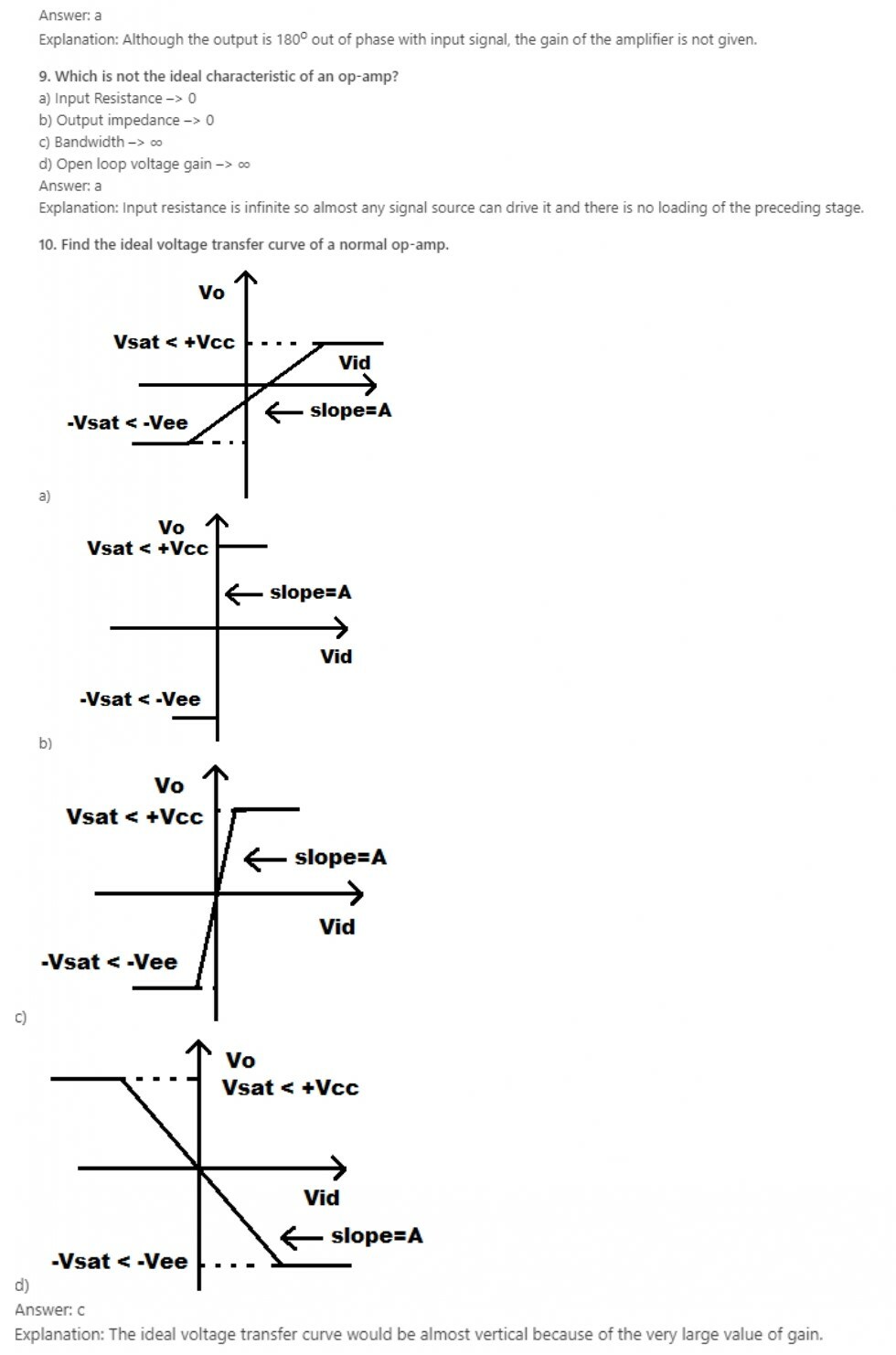
2. Which of the following electrical characteristics is not exhibited by an ideal op-amp?
a) Infinite voltage gain
b) Infinite bandwidth
c) Infinite output resistance
d) Infinite slew rate
Answer: c
Explanation: An ideal op-amp exhibits zero output resistance so that output can drive an infinite number of other devices.
3. An ideal op-amp requires infinite bandwidth because
a) Signals can be amplified without attenuation
b) Output common-mode noise voltage is zero
c) Output voltage occurs simultaneously with input voltage changes
d) Output can drive infinite number of device
Answer: a
Explanation: An ideal op-amp has infinite bandwidth. Therefore, any frequency signal from 0 to ∞ Hz can be amplified without attenuation.
4. Ideal op-amp has infinite voltage gain because
a) To control the output voltage
b) To obtain finite output voltage
c) To receive zero noise output voltage
d) None of the mentioned
Answer: b
Explanation: As the voltage gain is infinite, the voltage between the inverting and non-inverting terminal (i.e. differential input voltage) is essentially zero for finite output voltage.
15. In an ideal op-amp, which is not true?
a) Open loop voltage gain is infinite
b) Input resistance is infinite
c) Slew rate is infinite
d) CMRR is zero
Answer: d
Explanation: For an ideal op-amp, the open loop voltage gain is infinite. The output resistance is 0 and the input resistance is infinite. Op-amp has zero input current, zero offset voltage, infinite bandwidth, infinite CMRR and infinite slew rate.
16. A practical op-amp has a bandwidth of only 10 Hz. Gain is 106, and the required bandwidth is 100 kHz. How much feedback is required?
a) 0.99% negative feedback
b) 0.99% positive feedback
c) 1% negative feedback
d) 1% positive feedback
Answer: a
Explanation: B2 = B1(1+βA) = 10(1+β106) = 100k
1 + β106 = 10k
β = 9.999×10⁻³
In percentage, feedback β = 0.99% negative feedback.
17. Given that for an op-amp the gain is 103, the slew rate is 1.5V/μsec. Input is 5×10⁻³sinωt, calculate maximum frequency to prevent distortion.
a) 47.7 kHz
b) 0.3 MHz
c) 477 Hz
d) 3 kHz
Answer: a
Explanation: dVOUT(max)/dT =< Slew rate
A.Vmω =< 1.5 V/μsec
103.5.10-3.ω = < 1.5×10⁶
ω=<0.3×10⁶
Frequency f = 0.0477×10⁶Hz
18. Given that CMRR is 100dB. Input common-mode voltage is 12 V. Differential voltage gain is 4000. Calculate output common-mode voltage.
a) 48V
b) 0.48V
c) 20V
d) 11V
Answer: b
Explanation: CMRR = 20 log(AD/ACM) = 20 log(4000×12/Vocm) = 100
Log(48000/VOCM) = 5
48000/VOCM = 105
VOCM = 0.48V.
19. The unity gain bandwidth for an op-amp having open loop gain 2×10⁶ is 10 Mhz. Calculate the AC gain of op-amp at an input of 2000 Hz.
a) 2000
b) 5000
c) 10000
d) 12.5
Answer: b
Explanation: UGB = AOLfOL
fOL = 10M/2×106 = 5Hz
The AC gain |A| = AOL1+(f/5)2√
|A| = 2×10⁶/400 = 5000.
20. Given that:
A: Voltage gain of op-amp decreases at high frequencies
B: Its internal structure uses a capacitor
a) Both A and B are correct, and B is the correct reason for A
b) Both A and B are correct, but B is not the correct reason for A
c) A is correct and B is incorrect
d) A is incorrect and B is correct
Answer: a
Explanation: The internal structure of an op-amp uses a compensation capacitor for stability purpose. It provides dominant pole compensation; thereby the op-amp remains stable. However, the op-amp gain remains constant at low frequencies but decreases at high frequencies due to a compensation capacitor.
21. Till what frequency do we get amplification from IC 741?
a) Unity gain bandwidth
b) 3-dB frequency
c) Infinity
d) UGB + fOL
Answer: a
Explanation: The 3dB frequency is the cut-off frequency, where the gain is 12√ of the maximum. The gain is only constant for infinite frequency, that is, has infinite bandwidth if the op-amp is ideal, which practically doesn’t exist. The UGB is the point at which gain of op-amp reaches 1.
22. What is the use of the compensation capacitor in op-amp?
a) Improves the amplification of op-amp
b) Decreases the slew rate of op-amp
c) Increases the bandwidth of op-amp
d) Op-amp acts as all pass filter
Answer: b
Explanation: Compensation capacitor in the internal structure of op-amp to improve its frequency response, increasing its stability. It also decreases the slew rate of the op-amp.
23. Which is not the internal circuit of operational amplifier?
a) Differential amplifier
b) Level translator
c) Output driver
d) Clamper
Answer: d
Explanation: Clamper is an external circuit connected at the output of Operational amplifier, which clamp the output to desire DC level.
24. The purpose of level shifter in Op-amp internal circuit is to
a) Adjust DC voltage
b) Increase impedance
c) Provide high gain
d) Decrease input resistance
Answer: a
Explanation: The gain stages in Op-amp are direct coupled. So, level shifter is used for adjustment of DC level.
25. How a symmetrical swing is obtained at the output of Op-amp
a) Providing amplifier with negative supply voltage
b) Providing amplifier with positive voltage
c) Providing amplifier with positive& negative voltage
d) None of the mentioned
Answer: c
Explanation: For example, consider a single voltage supply +15v. During positive half cycle the output will be +5v and -10v during negative half cycle.
Therefore, the maximum peak to peak output swing, -5v (-10v) = -15v (Asymmetrical swing).
So, to get symmetrical swing both positive and negative supply voltage with bias point fixed suitably is required.
26. What is the purpose of differential amplifier stage in internal circuit of Op-amp?
a) Low gain to differential mode signal
b) Cancel difference mode signal
c) Low gain to common mode signal
d) Cancel common mode signal
Answer: d
Explanation: Any undesired noise, common to both of the input terminal is suppressed by differential amplifier.
27. Which of the following is not preferred for input stage of Op-amp?
a) Dual Input Balanced Output
b) Differential Input Single ended Output
c) Cascaded DC amplifier
d) Single Input Differential Output
Answer: c
Explanation: Cascaded DC amplifier suffers from major problem of drift of the operating point, due to temperature dependency of the transistor.
28. What will be the emitter current in a differential amplifier, where both the transistor are biased and matched? (Assume current to be IQ)
a) IE = IQ/2
b) IE = IQ
c) IE = (IQ)2/2
d) IE = (IQ)2
Answer: a
Explanation: Due to symmetry of differential amplifier circuit, current IQ divides equally through both transistors.
31. For Vd > ±4VT, the function of differential amplifier will be
a) Switch
b) Limiter
c) Automatic gain control
d) Linear Amplifier
Answer: b
Explanation: At this condition, input voltage of the amplifier is greater than ±100mv and thus acts as a limiter.
32. Change in value of common mode input signal in differential pair amplifier make
a) Change in voltage across collector
b) Slight change in collector voltage
c) Collector voltage decreases to zero
d) None of the mentioned
Answer: a
Explanation: In differential amplifier due to symmetry, both transistors are biased and matched. Therefore, Voltage at each collector will be same.
34. A differential amplifier has a transistor with β0= 100, is biased at ICQ = 0.48mA. Determine the value of CMRR and ACM, if RE =7.89kΩ and RC = 5kΩ.
a) 49.54 db
b) 49.65 d
c) 49.77 db
d) 49.60 db
Answer: b
Explanation: Differential mode gain, ADM= -gmRC and Common mode gain,
⇒ ACM= -(gmRC)/(1+2gmRE)
(for β0≫1).
Substituting the values,
⇒ gm= ICQ/VT = 0.48mA/25mv=19.2×10-3Ω-1
⇒ ADM= -gm×RC= -19.2×10⁻³Ω-1×5kΩ= -96
⇒ ACM= -(gmRC)/(1+2gmRE)= -(19.2×10⁻³Ω-1×5kΩ) /(1+2×-⇒ 19.2×10⁻³Ω-1×7.89kΩ) = -0.3158
CMRR = -96/-0.3158= 303.976
=20log303.976
=49.65db
35. The opamp in the Inverting circuit is in __________
a) Linear region
b) Saturation
c) Cut-off region
d) Non-linear region
Answer: a
Explanation: We assume that the opamp is in linear region.
36. In an Inverting Amplifier circuit, the output voltage vo is expressed as a function of ____________
a) Input current
b) Output current
c) Source voltage
d) Source current
Answer: c
Explanation: The goal of an inverting circuit is to express output voltage vo as a function of source voltage vs.
37. The other name for Gain is ____________
a) Scaling factor
b) Output
c) Amplifying factor
d) Scaling level
Answer: a
Explanation: The gain is also known as scaling factor and it is the ratio of Rf/Rs in case of an Inverting amplifying circuit.
38. If VCC = 12V and vs=1mV, then Rf/Rs is _____________
a) >12000
b) <12000
c) 12000
d) 1
Answer: b
Explanation: Rf/Rs ≤ │VCC/vs│.
39. In the expression vo= -Avn, A is called ______________
a) Closed loop gain
b) Closed loop fault
c) Open loop fault
d) Open loop gain
Answer: d
Explanation: A is called open loop gain.
40. The circuits of an inverting and Non-Inverting amplifying comprises of __________ and _______ number of resistors.
a) 3, 2
b) 2, 3
c) 2, 2
d) 3, 3
Answer: b
Explanation: Inverting amplifying circuit- Rs, Rf.
Non-Inverting amplifying circuit – Rs, Rf, Rg.
41. The condition for a Non-inverting amplifying circuit to operate in linear region operation _____________
a) (Rs+Rf)/Rs < │VCC/vg│
b) (Rs+Rf)/Rs ≠ │VCC/vg│
c) (Rs+Rf)/Rs > │VCC/vg│
d) (Rs+Rf)/Rs = │VCC/vg│
Answer: a
Explanation: Assume that opamp is ideal. The condition for the linear region operation in a Non-inverting amplifying circuit is (Rs+Rf)/Rs <│VCC/vg│.
42. If Rs= 3Ω, Rf= 6Ω then the relation between vo and vg in case of a Non-Inverting amplifying circuit.
a) vo= 9vg
b) vo= 6vg
c) vo= 3vg
d) vo= vg
Answer: c
Explanation: vo= ((Rs+Rf)/Rs) *vg.
43. If Rs= 5Ω, Rf= 25Ω and -2.5V ≤ vg ≤ 2.5V. What are the smallest power supply voltages that could be applied and still have opamp in linear region?
a) ±9V
b) ±2.5V
c) ±6V
d) ±15V
Answer: d
Explanation: vo= ((Rs+Rf)/Rs) *vg. By substituting the values, we have vo=6vg.
vo=6(-2.5) = -15
vo=6(2.5) =15.
44. If an inverting amplifying circuit has a gain of 10 and ±15V power supplies are used. The values of input for which opamp would be in the linear region?
a) ±1.25
b) ±1.5V
c) ±2.25
d) ±0.5
Answer: b
Explanation: Gain= Rf/Rs= 10 and vo= (-Rf/Rs)*vs.
→ vo= -10vs and given -12V≤ vo ≤ 12V.
→ -15= -10vs. So, vs= 1.5V
→ 15=-10vs. So, vs=-1.5V.
45. If the gain of an inverting amplifying circuit is 13 and ±22V power supplies are used. What range of input values allows the opamp to be in linear region?
a) ±1.69
b) ±1.35V
c) ±2.28
d) ±0.5
Answer: a
Explanation: Gain= Rf/Rs= 13 and vo= (-Rf/Rs)*vs.
→ vo= -13vs and given -22V≤ vo ≤ 22V.
→ -22= -13vs. So, vs=1.692 V
→ 22=-13vs. So, vs=-1.692V.
48. In the non-inverting configuration of operational amplifier
a) The positive terminal is connected to the ground directly
b) The negative terminal is connected to the ground directly
c) The positive terminal is connected to the power source
d) The negative terminal is connected to the power source
Answer: c
Explanation: Non inverting configuration requires a power source connected to the power source.
49. For ideal non-inverting operational amplifier
a) Input and output resistances are infinite
b) Input resistance is infinite and output resistance is zero
c) Input resistance is zero and output resistance is infinite
d) Input and output resistances are zero
Answer: b
Explanation: It is an ideal characteristic of the non-inverting op amp.
50. For an ideal non-inverting operational amplifier having finite gain (A), the ratio of output voltage (v0) to input voltage (vi) is (given R2 is the feedback resistance)
a) (1+R2/R1)/(1+((1+R2/R1)/A))
b) (R2/R1)/(((1+R2/R1)/A))
c) (1+R2/R1)/(((1+R2/R1)/A))
d) (R2/R1)/(1+((1+R2/R1)/A))
Answer: a
Explanation: It is a standard mathematical expression.
51. The gain for an ideal non-inverting operational amplifier is (given R2 is the feedback resistance)
a) R2/R1 – 1
b) R2/R1
c) -R2/R1
d) R2/R1 + 1
Answer: d
Explanation: It is a standard mathematical expression.
52. While performing an experiment to determine the gain for an ideal operational amplifier having finite gain, a student mistakenly used the equation 1 + R2/R1 where R2 is the feedback resistance. What is the percentage error in his result? Given A is the finite voltage gain of the ideal amplifier used.
a) (R2/R1)/(A+ R2/R1) X 100%
b) (1+R2/R1)/(A+R2/R1) X 100%
c) (1+R2/R1)/(A+1+R2/R1) X 100%
d) (R2/R1)/(A+1+R2/R1) X 100%
Answer: c
Explanation: The correct formula is (1+R2/R1)/(1+((1+R2/R1)/A)).
53. The finite voltage gain of a non-inverting operational amplifier is A and the resistance used is R1 and R2 in which R2 is the feedback resistance. Under what conditions it can one use the expression 1 + R2/R1 to determine the gain of the amplifier?
a) A ~ R2/R1
b) A >> R2/R1
c) A << R2/R1
d) None of the mentioned
Answer: b
Explanation: The formula is valid for the ideal case in which the value of A is infinite, practically it should be very large when compared to R2/R1 .
54. Which of the following is not true for a voltage follower amplifier?
a) Input voltage is equal to output voltage
b) Input resistance is infinite and output resistance is zero
c) It has 100% negative feedback
d) None of the mentioned
Answer: d
Explanation: All the statements are false.
55. For designing a non-inverting amplifier with a gain of 2 at the maximum output voltage of 10 V and the current in the voltage divider is to be 10 μA the resistance required are R1 and R2 where R2 is used to provide negative feedback. Then
a) R1 = 0.5 MΩ and R2 = 0.5 MΩ
b) R1 = 0.5 kΩ and R2 = 0.5 kΩ
c) R1 = 5 MΩ and R2 = 5 MΩ
d) R1 = 5 kΩ and R2 = 5 kΩ
Answer: a
Explanation: 1 + R2/R1 = 2 and 10/(R1+R2) = 10 μA. Solve for R1 and R2.
56. It is required to connect a transducer having an open-circuit voltage of 1 V and a source resistance of 1 MΩ to a load of 1-kΩ resistance. Find the load voltage if the connection is done (a) directly and (b) through a unity-gain voltage follower.
a) 1 μV and 1 mV respectively
b) 1 mV and 1 V respectively
c) 0.1 μV and 0.1 mV respectively
d) 0.1 mV and 0.1 V respectively
Answer: b
Explanation: When a unity gain follower is uses then input signal is equal to output signal. When connected directly, output signal is given by 1 X 1kΩ/1MΩ or 1mV.
58. In which amplifier the output voltage is equal to the negative sum of all the inputs?
a) Averaging amplifier
b) Summing amplifier
c) Scaling amplifier
d) All of the mentioned
Answer: b
Explanation: In summing amplifier the output voltage is equal to the sum of all input. Since the total input is a sum of negative input, the amplifier is an inverting summing amplifier.
59. Determine the expression of output voltage for inverting summing amplifier consisting of four internal resistors? (Assume the value of internal resistors to be equal)
a) Vo = -(Rf/R )×(Va +Vb+Vc+Vd)
b) Vo = (RF/R)×(Va +Vb+Vc+Vd)
c) Vo = (R/ RF)×(Va +Vb+Vc+Vd)
d) None of the mentioned
Answer: a
Explanation: If the internal resistors of the circuit is same i.e Ra=Rb=Rc=Rd=R (since there are four internal resistor)
Then, the output voltage for inverting amplifier is given as Vo= -(Rf/R)×(Va +Vb+Vc+Vd).
60. An inverting amplifier with gain 1 have different input voltage: 1.2v,3.2v and 4.2v. Find the output voltage?
a) 4.2v
b) 8.6v
c) -4.2v
d) -8.6v
Answer: d
Explanation: When the gain of the inverting summing amplifier gain is 1 then, the internal resistors and feedback resistors have the same value. So, the output is equal to the negative sum of all input voltages.
VO= -(Va+Vb+Vc) =-(1.2+3.2+4.2)= -8.6v.
61. In which type of amplifier, the input voltage is amplified by a scaling factor
a) Summing amplifier
b) Averaging amplifier
c) Weighted amplifier
d) Differential amplifier
Answer: c
Explanation: The weighted amplifier is also called as scaling amplifier. Here each input voltage is amplified by a different factor i.e. Ra,Rb and Rc are different in values ( which are the input resistors at each input voltage).
62. An inverting scaling amplifier has three input voltages Va, Vb and Vc. Find it output voltage?
a) VO= – {[(RF/Ra)×Va] +[(RF/Rb)×Vb]+[(RF/Rc)×Vc]}
b) VO= – [(RF/Ra)+(RF/Rb)+(RF/Rc)]×[( Va +Vb+Vc)].
c) VO = – {[(Ra/RF)×Va] +[(Rb/RF)×Vb]+[(Rc/RF)×Vc]}
d) None of the mentioned
Answer: a
Explanation: Since three input voltages are given assume the input resistors to be Ra,Rb and Rc. In a scaling amplifier, the input voltages are amplified by a different factor
=> ∴ RF/Ra ≠ RF/Rb ≠ RF/Rc
Therefore, output voltage Vo = -{[(RF/Ra) Va] +[(RF/Rb) Vb]+[(RF/Rc) Vc]}.
63. An amplifier in which the output voltage is equal to average of input voltage?
a) Summing amplifier
b) Weighting amplifier
c) Scaling amplifier
d) Averaging amplifier
Answer: d
Explanation: An averaging amplifier can be used as an averaging circuit, in which the output voltage is equal to the average of all the input voltages.
64. Find out the gain value by which each input of the averaging amplifier is amplified ?( Assume there are four inputs)
a) 0.5
b) 0.25
c) 1
d) 2
Answer: b
Explanation: In an averaging amplifier, the gain by which each input is amplified must be equal to lower number of input.
=> RF /R =1/n , where n=number of inputs
∴ RF /R=1/4 = 0.25 (Four inputs)
So, each input in the averaging amplifier must be amplified by 0.25.
65. 3v, 5v and 7v are the three input voltage applied to the inverting input terminal of averaging amplifier. Determine the output voltage?
a) -5v
b) -10v
c) -15v
d) -20v
Answer: a
Explanation: The output voltage, Vo = -[(Va+Vb+Vc)/3] = -[(3+5+7)/3] =-5v.
67. Which type of amplifier has output voltage equal to the average of all input voltages?
a) Inverting averaging amplifier
b) Non-inverting averaging amplifier
c) Non-inverting summing amplifier
d) Inverting scaling amplifier
Answer: b
Explanation: In non-inverting averaging amplifier, the non-inverting input voltage is the average of all inputs, with a positive sign.
68. Expression for output voltage of non-inverting summing amplifier with five input voltage?
a) Vo = 5×( Va + Vb+ Vc+ Vd+ Ve)
b) Vo = [1+( Rf/R1)]× ( Va + Vb+ Vc+ Vd+ Ve)
c) Vo = Va + Vb+ Vc+ Vd+ Ve
d) Vo = ( Va + Vb+ Vc+ Vd+ Ve) /5
Answer: c
Explanation: The output voltage of non-inverting summing amplifier is (1+ ( Rf / R1 )) times the average of all input voltages in the circuit.
Since there are five input voltages => (1+ ( Rf / R1 )) =5
Therefore, Vo = 5×( Va + Vb+ Vc+ Vd+ Ve) /5
=> Vo = (Va + Vb+ Vc+ Vd+ Ve).
70. If the gain of a non-inverting averaging amplifier is one, determine the input voltages if the output voltage, if the output voltage is 3v?
a) V1 =6v ,V2=3v and V3=2v
b) V1 =9v ,V2=5v and V3=-4v
c) V1 =8v ,V2=-6v and V3=1v
d) V1 =7v ,V2=4v and V3=-3v
Answer: d
Explanation: As the output voltage = Average of all input voltage = sum of input voltage /3
∴ sum of input voltage =3×3=9.
From the given option, the combination of input voltage 7v, 4v and -3v gives the value 9v.
72. Find the type of amplifier that cannot be constructed in differential configuration?
a) Summing amplifier
b) Scaling amplifier
c) Averaging amplifier
d) Subtractor
Answer: c
Explanation: In differential op-amp configuration, an amplifier produces sum or difference between two input terminals of op-amp. So, averaging is not possible in this type of configuration.
73. Calculate the output voltage, when a voltage of 12mv is applied to the non-inverting terminal and 7mv is applied to inverting terminal of a subtractor.
a) 19mv
b) 5mv
c) 1.7mv
d) 8.4mv
Answer: b
Explanation: Output voltage of a subtractor Vo = Vnon-inverting terminal – Vinverting terminal = 12mv-7mv =5mv.
76. The output voltage of a summing amplifier is equal to (assume sum of input voltage as Vn )
a) Vn (non-inverting terminal)+ Vn (inverting terminal)
b) Vn (non-inverting terminal)+ (-Vn (inverting terminal)
c) -Vn (non-inverting terminal)+ (-Vn (inverting terminal)
d) -Vn (non-inverting terminal)+ Vn (inverting terminal)
Answer: b
Explanation: The output voltage of summing amplifier is equal to sum of the input voltage applied to the non-inverting terminal plus the negative sum of the input voltage applied to the inverting terminal.
77. Why differential amplifiers are preferred for instrumentation and industrial applications?
a) Input resistance is low
b) Produce amplified output
c) Amplify individual input voltage
d) Reject common mode voltage
Answer: d
Explanation: Differential amplifiers are preferred in these applications because they are better able to reject common-mode voltage than single input circuits and present balanced input impedance.
78. Which of the following is a combination of inverting and non-inverting amplifier?
a) Differential amplifier with one op-amp
b) Differential amplifier with two op-amps
c) Differential amplifier with three op-amps
d) Differential amplifier with four op-amps
Answer: a
Explanation: In differential amplifier with one op-amp both the inputs are connected to separate voltage source. So, if any one of the source is reduced to zero, differential amplifier acts as an inverting or non-inverting amplifier.
79. What will be the output voltage when Vx =0v?
(Where Vx –> inverting input terminal of differential amplifier with one op-amp)
a) Vo = -(1+R F/R1)*V1
b) Vo = -(1- R F/ R1)*V1
c) Vo = (1+ R F/ R1)*V1
d) Vo = (R F/ R1)*V1
Answer: c
Explanation: When Vx =0v, the configuration is a non-inverting amplifier.
81. Compute the output voltage if the input voltage is reduced to zero in differential amplifier with one op-amp?
a) Inverted Voltage
b) Same as the input voltage
c) Amplified inverted voltage
d) Cannot be determined
Answer: d
Explanation: It is not mentioned clearly whether inverting input or non-inverting input is reduced to zero. Therefore, the output cannot be determined.
82. The difference between the input and output voltage are -1v and 17v. Calculate the closed loop voltage gain of differential amplifier with one op-amp?
a) -51
b) 34
c) -17
d) 14
View Answer
Answer: c
Explanation: Voltage gain of differential amplifier with one op-amp, AD=Output voltage / Difference of input voltage
=> AD = 17v/-1v = -17v.
84. The gain of differential amplifier with one op-amp is same as that of
a) The inverting amplifier
b) The non-inverting amplifier
c) Both inverting and non-inverting amplifier
d) None of the mentioned
Answer: a
Explanation: The gain of differential amplifier is given as AD= -(RF /R1), which is equivalent to the output voltage obtained from the inverting amplifier.
85. Find the value of input resistance for differential amplifier with one op-amp. If R1 = R2=100Ω and RF = R3 =5kΩ.
a) RIFx = 110Ω; RIFy = 6.7kΩ
b) RIFx = 100Ω; RIFy = 5.1kΩ
c) RIFx = 150Ω; RIFy = 7.2kΩ
d) RIFx = 190Ω; RIFy = 9.0kΩ
Answer: b
Explanation: The input resistance of inverting amplifier is RIFx = (R1) and the input resistance of non-inverting amplifier is RIFy = (R2+ R3)
=> ∴ RIFx = 100Ω and
=> RIFy =100+5kΩ =5.1kΩ.
86. What is the net output voltage for differential amplifier with one op-amp
a) Vo = -(RF /R1)*Vx
b) Vo = -(RF /R1)*(Vx -Vy)
c) Vo = (1+RF /R1)*(Vx -Vy)
d) None of the mentioned
Answer: b
Explanation: The net output voltage for differential amplifier with one op-amp is given as Vo= -(RF /R1)*(Vx-Vy).
1. What we use for impedance matching in RF amplifiers?
a) RC coupling
b) Transformer coupling
c) Direct coupling
d) RF coupling
Answer: b
Explanation: Impedance matching is the input impedance of an electrical load or the output impedance of corresponding electrical signal source to maximize power transfer or minimize signal reflection from the load. Transformer coupling is basically used for impedance matching in RF amplifiers. It is usually used with a small load for power amplification.
2. Neutralization cancels unwanted feedback by bypassing the feedback to the neutral or ground plane.
a) True
b) False
Answer: b
Explanation: Neutralization cancels unwanted feedback by adding feedback out of phase with the unwanted feedback. It is a method of filtering noise out of signals.
3. In a receiver, distortion can occur in ________
a) Mixer
b) Detector
c) IF amplifiers
d) Either mixer or detector or IF amplifiers
Answer: d
Explanation: Distortion in a receiver can occur in either mixer or in the detector. It can also occur in IF amplifiers. Distortion is the change in the shape of the waveform.
4. How we limit the response of a receiver to a weak signal?
a) by the AGC
b) by the noise that is generated in the receiver
c) by the dynamic range of the receiver
d) by the type of detector circuit being used
Answer: b
Explanation: The response of a receiver to weak signals is limited by the noise. This noise is generated in the receiver only. Noise is the unwanted signal that is present in the passband of the signal.
5. When aliasing will take place?
a) Sampling signals less than Nyquist Rate
b) Sampling signals more than Nyquist Rate
c) Sampling signals equal to Nyquist Rate
d) Sampling signals at a rate which is twice of Nyquist Rate
Answer: a
Explanation: Aliasing causes different signals to become indistinguishable when sampled. It happens when the sampling rate is less than Nyquist rate. To prevent aliasing, sampling signals should be at a rate which is twice of Nyquist Rate.
6. A resonant circuit is a simple form of bandpass filter.
a) True
b) False
Answer: a
Explanation: The quality factor Q, of a resonant circuit is a measure of quality of resonant circuit, thus indicating the performance of the resonant circuit. Bandwidth can be seen as the ratio of the resonant frequency to quality factor. A higher value for Q means a more narrow bandwidth, which we want in many applications.
7. Which statement is true for high level amplitude modulation?
a) all RF amplifiers are of class A
b) all RF amplifiers can be nonlinear
c) minimum RF power is required
d) maximum RF power is required
Answer: b
Explanation: In high level AM, modulation is done at high power of carrier and modulating signal therefore output power is high. Therefore, power amplifiers are not used to boost the carrier and modulating signal. Thus, all RF amplifiers are non-linear.
8. Which statement is true for low level amplitude modulation?
a) all RF amplifiers are of class A
b) all RF amplifiers can be linear
c) minimum RF power is required
d) maximum RF power is required
Answer: b
Explanation: For low level AM, modulation is done at low power of carrier and modulating signal, so power amplifiers are used to boost the carrier and modulating signal. Therefore, output power is low. Thus, the amplifiers used are linear.
9. Which two networks can be used for impedance matching?
a) pi network and T network
b) pi network and bridge network
c) bridge network and T network
d) pi network and omega network
Answer: a
Explanation: If a source with low impedance is connected with a load with high impedance then the power that can pass through the connection is limited by higher impedance. Generally the two networks, pi and T are used for impedance matching.
10. Which statement is true about frequency multipliers?
a) they are essentially balanced modulators
b) they are essentially class C amplifiers
c) they are essentially class AB amplifiers
d) they are essentially mixers
Answer: b
Explanation: Frequency multiplier multiplies the frequency of the input by an integer, such that the output is a multiple of the input. Frequency multipliers are generally class C amplifiers.
11. In Amplitude Modulation, the instantaneous values of the carrier amplitude changes in accordance with the amplitude and frequency variations of the modulating signal.
a) True
b) False
Answer: a
Explanation: In Amplitude Modulation, the amplitude of the carrier sine wave is varied by the value of the information signal. The instantaneous value of the carrier amplitude changes in accordance with the amplitude and frequency variations of the modulating signal. The carrier frequency remains constant during the modulation process, But its amplitude varies in accordance with the modulating signal.
12. What is the line connecting the positive and negative peaks of the carrier waveform called?
a) Peak line
b) Maximum amplitude ceiling
c) Modulation index
d) Envelope
Answer: d
Explanation: An imaginary line connecting the positive peaks and negative peaks of the carrier waveform gives the exact shape of the modulating information signal. This line is known as the envelope.
13. What is the reference line for the modulating signal?
a) Zero line
b) Carrier peak line
c) Modulated peak line
d) Un-modulated peak line
Answer: b
Explanation: The modulating signal uses the peak value of the carrier rather than zero as its reference point. The envelope varies above and below the peak carrier amplitude. The zero reference line of the modulating signal coincides with the peak value of the unmodulated carrier.
14. What happens when the amplitude of the modulating signal is greater than the amplitude of the carrier?
a) Decay
b) Distortion
c) Amplification
d) Attenuation
Answer: b
Explanation: The zero reference line of the modulating signal coincides with the peak value of the unmodulated carrier. Because of this, the relative amplitudes of the carrier and modulating signal are important. When the amplitude of the modulating signal is greater than the amplitude of the carrier, distortion will occur.
15. What is the effect of distortion?
a) Total information loss
b) Error information
c) Attenuated information
d) Amplified information
Answer: b
Explanation: Distortion occurs when the modulating signal amplitude is greater than the amplitude of the carrier, causing incorrect information to be transmitted. In amplitude modulation, it is particularly important that the peak value of the modulating signal be less than the peak value of the carrier.
16. What is the circuit used for producing AM called?
a) Modulator
b) Transmitter
c) Receiver
d) Duplexer
Answer: a
Explanation: The circuit used for producing AM is called a modulator. It has two inputs, the carrier and the modulating signal, and the resulting output is the modulated signal. Amplitude modulators compute the product of the carrier and modulating signals.
17. The ratio between the modulating signal voltage and the carrier voltage is called?
a) Amplitude modulation
b) Modulation frequency
c) Modulation index
d) Ratio of modulation
Answer: c
Explanation: For undistorted modulation to occur, the voltage of modulating signal Vm must be less than the carrier voltage Vc. Therefore, the relationship between the amplitude of the modulating signal and the amplitude of the carrier signal is important. This relationship, known as the modulation index m, is the ratio m = Vm⁄Vc.
18. What is the percentage of modulation if the modulating signal is of 7.5V and carrier is of 9V?
a) 100
b) 91
c) 83.33
d) 0
Answer: c
Explanation: modulation index m = Vm⁄Vc = 7.5⁄9* 100 = 83.33.
19. When does over-modulation occur?
a) Modulating signal voltage < Carrier voltage
b) Modulating signal voltage > Carrier voltage
c) Modulating signal voltage = Carrier voltage
d) Modulating signal voltage =0
Answer: b
Explanation: Over-modulation is a condition in which the modulating signal voltage is much greater than the carrier voltage. The received signal will produce an output waveform in the shape of the envelope, whose negative peaks have been clipped off.
20. What is the condition for greatest output power at the transmitter without distortion?
a) Modulating signal voltage > Carrier voltage
b) Modulating signal voltage < Carrier voltage
c) Modulating signal voltage = Carrier voltage
d) Modulating signal voltage = 0
Answer: c
Explanation: When the modulation index is 1 or the percentage of modulation is 100, modulating signal voltage is equal to the carrier voltage. This results in the greatest output power at the transmitter and the greatest output voltage at the receiver, with no distortion.
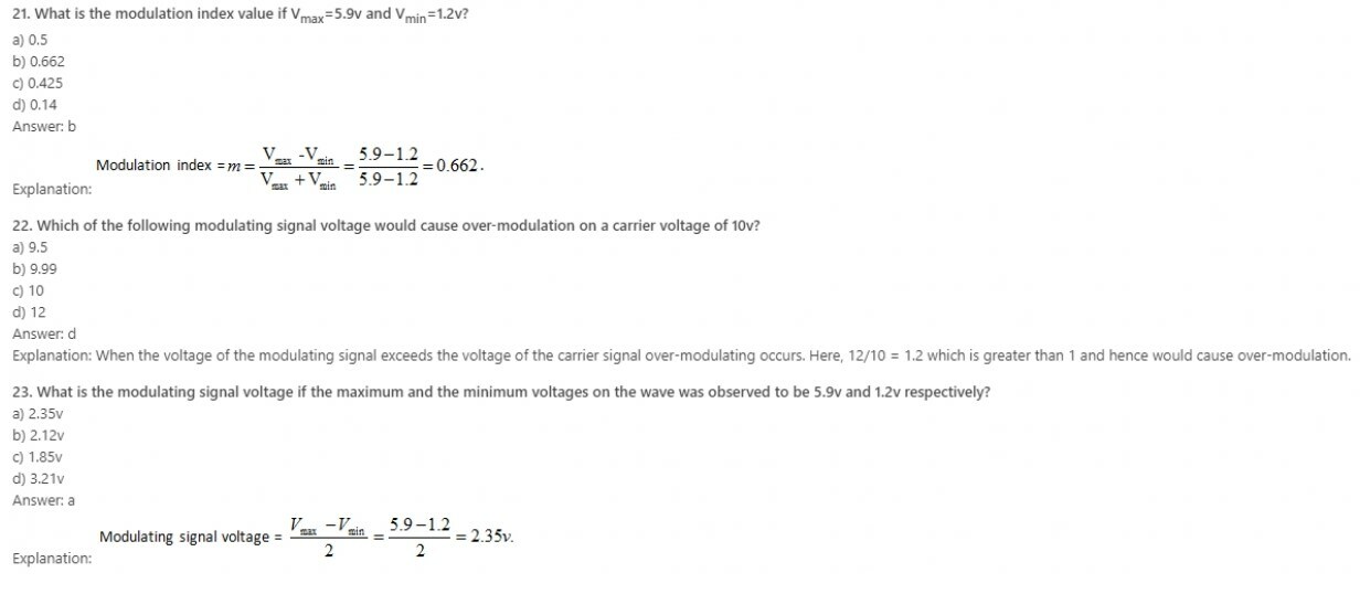
24. Carrier signal in modulation technique is _______ signal.
a) High frequency
b) Low frequency
c) High amplitude
d) Low amplitude
Answer: a
Explanation: Carrier signal in modulation technique is a high frequency signal. In amplitude modulation, the amplitude of a high frequency carrier signal is varied in accordance to the instantaneous amplitude of the modulating signal.
25. Modulation index of an AM signal is ratio of __________ to the _______
a) Peak carrier amplitude, Peak message signal amplitude
b) Peak message signal amplitude, Peak carrier amplitude
c) Carrier signal frequency, Message signal frequency
d) Message signal frequency, Carrier signal frequency
Answer: b
Explanation: The modulation index k of an AM signal is defined as the ratio of the peak message signal amplitude to the peak carrier amplitude. The modulation index is often expressed as a percentage. It is also called percentage modulation.
26. If the peak message signal amplitude is half the peak amplitude of the carrier signal, the signal is _____ modulated.
a) 100%
b) 2%
c) 50%
d) 70%
Answer: c
Explanation: The modulation is also expressed in percentage. It is also called percentage modulation. The signal is said to be 50% modulated if the peak message signal amplitude is half the peak amplitude of the carrier signal.
27. A percentage of modulation greater than ___________ will distort the message signal.
a) 10%
b) 25%
c) 50%
d) 100%
Answer: d
Explanation: A percentage of modulation greater than 100% will distort the message signal if detected by an envelope detector. In this case the lower excursion of the signal will drive the carrier amplitude below zero, making it negative (and hence changing its phase).
28. The RF bandwidth of AM is ____________ the maximum frequency contained in the modulating message signal.
a) Equal
b) Two times
c) Four times
d) Ten times
Answer: b
Explanation: The RF bandwidth of an AM signal is equal to BAM=2fm. It is double the maximum frequency contained in the modulating message signal. AM spectrum consists of an impulse at the carrier frequency and two sidebands which replicate the message spectrum.
29. Single sideband AM systems occupy same bandwidth as of conventional AM systems.
a) True
b) False
Answer: b
Explanation: Single sideband (SSB) AM systems transmit only one of the sidebands (either upper or lower) about the carrier. Hence, they occupy only half the bandwidth of conventional AM systems.
30. How is the performance of SSB AM systems in fading channels?
a) Poor
b) Best
c) Good
d) Average
Answer: a
Explanation: SSB systems have the advantage of being very bandwidth efficient. But their performance in fading channels is very poor. For proper detection, the frequency of the oscillator at the product detector mixer in the receiver must be same as that of the incoming carrier frequency.
31. Which of the following is a disadvantage of tone-in-band SSB system?
a) High bandwidth
b) Bad adjacent channel protection
c) Effects of multipath
d) Generation and reception of signal is complicated
Answer: d
Explanation: Tone-in-band SSB systems has the advantage of maintaining the low bandwidth property of the SSB signals, while at the same time providing good adjacent channel protection. The tone in band system employs feedforward automatic gain and frequency control to mitigate the effects of multipath induced fading.
32. FFSR in AM systems stands for ________
a) Feedforward signal regeneration
b) Feedbackward signal regeneration
c) Feedbackward system restoration
d) Feedforward system restoration
Answer: a
Explanation: FFSR stands for Feedforward signal regeneration. If the pilot tone and the information bearing signal undergo correlated fading, it is possible at the receiver to counteract the effects of fading through signal processing based on tracking of pilot tone. This process is called FFSR.
33. AM demodulation technique can be divided into _____ and _____ demodulation.
a) Direct, indirect
b) Slope detector, zero crossing
c) Coherent, noncoherent
d) Quadrature detection, coherent detection
Answer: c
Explanation: AM demodulation techniques may be broadly divide into two main categories. They are called coherent and noncoherent demodulation. They are differentiated by the knowledge of transmitted carrier frequency and phase at the receiver.
34. Non coherent detection requires the knowledge of transmitted carrier frequency and phase at the receiver.
a) True
b) False
Answer: b
Explanation: Non coherent detection does require the knowledge of phase information. However, coherent detection requires knowledge of the transmitted carrier frequency and phase at the receiver.
35. A product detector in AM systems is also called ___________
a) Envelope detector
b) Differentiator
c) Integrator
d) Phase detector
Answer: d
Explanation: A product detector is also called a phase detector. It forms a coherent demodulator for AM signals. It is a down converter circuit which converts the input bandpass signal to a baseband signal.
36. AM system use only product detector for demodulation. They never use envelope detectors.
a) True
b) False
Answer: b
Explanation: AM systems can use either product detector or envelope detector for demodulation. As a rule, envelope detectors are useful when input signal power is at least 10dB greater than noise power, whereas product detectors are able to process the AM signals with input signal to noise ratios well below 0 dB.
37. LCD uses ________
a) sematic crystals
b) twisted nematic crystals
c) nematic crystals
d) cholesteric crystals
Answer: b
Explanation: LCD uses liquid crystal display. It uses twisted nematic crystals which are a type of liquid crystal, consisting of a substance called the nematic. The nematic liquid crystal is placed between two plates of polarized glass.
38. Which of the following stage is present in FM receiver but not in AM receiver?
a) Amplitude limiter
b) Demodulator
c) AM amplifier
d) Mixer
Answer: a
Explanation: Amplitude Limiter circuit is used in FM receiver to remove the noise or any variation in amplitude present in the received signal. Thus, the output of the amplitude limiter has a constant amplitude. So it is only used in frequency modulation and not in amplitude modulation.
39. Function of duplexer in a RADAR is to permit the use of same antenna for transmission and reception.
a) True
b) False
Answer: a
Explanation: A duplexer is being an electronic unit, allows bi-directional communication over the same path. The transmitter and receiver can communicate simultaneously. In radar, the duplexer isolates the receiver from the transmitter while allowing them to share a common antenna.
40. Single Sideband Modulation (SSB) is generally reserved for point-to-point communication.
a) True
b) False
Answer: a
Explanation: A point-to-point communication refers to bidirectional communication between only one transmitter and one receiver. In SSB-SC modulation technique, the carrier is suppressed and only one of the two side-bands are transmitted. Thus, it reduces power consumption and lessens bandwidth. Thus, it is preferred for point-to-point communication.
41. For an AM transmitter, class C amplifier can be used after the modulation stage.
a) True
b) False
Answer: b
Explanation: In an AM transmitter, the required transmission power is obtained from class C amplifier, as it is a power amplifier, for low-level or high-level modulation. So it is not used after the modulation stage.
42. For which of the modulated system, the linear amplified modulated stage is used?
a) low level amplitude modulated system
b) high level amplitude modulated system
c) high level frequency modulated system
d) low level frequency modulated system
Answer: a
Explanation: In low-level modulation, the generation of amplitude modulated signal takes place at low power levels. The generated AM signal is then amplified using a chain of linear amplifiers, which are required to avoid waveform distortion. Thus, linear amplified modulated stage is used in low level amplitude modulated system.
43. When noise is passed through a narrow band filter, the output of filter should be?
a) triangular
b) square
c) parabolic
d) sinusoidal
Answer: d
Explanation: Narrow band filter is used to isolate a narrow band of frequencies from a wider bandwidth signal. It is a combination of band pass and band reject filter. When noise gets passed through it, the output of it should be sinusoidal.
44. A narrow band noise can exist in _________
a) AM only
b) PCM only
c) FM only
d) AM and FM both
Answer: d
Explanation: Narrow band filter is used to isolate a narrow band of frequencies from a wider bandwidth signal. It is a combination of band pass and band reject filter. So it can be used in both AM and FM to pass a band of frequencies or to attenuate a band of frequencies.
45. The upper and lower sideband frequencies for 5KHz amplitude modulation with a 30KHz carrier frequency will be?
a) 35KHz and 25KHz
b) 34KHz and 24KHz
c) 25KHz and 35KHz
d) 0.35KHz and 0.25KHz
Answer: a
Explanation: Upper sideband frequency will be (30 + 5) = 35 KHz and Lower sideband frequency will be (30 – 5) = 25 KHz.
46. Phase array radar can track many targets together.
a) True
b) False
Answer: a
Explanation: A phased array radar is an array of radiating elements, with each having a phase-shifter. The phase of the signal being emitted from the radiating element is changed to produce beams, thereby producing constructive or destructive interference for steering the beams in the required direction. Thus, it can track many targets together.
47. What do you understand by the term SSB?
a) Suppressed Side Band
b) Single Side Band
c) Suppressed Single Band
d) Selected Single Band
Answer: b
Explanation: SSB stands for Single Side band. In SSB-SC (Single Side Band Suppressed Carrier), the carrier is suppressed and only either of the two sidebands is transmitted. This reduces power consumption and also lessens the bandwidth.
48. SSB is a standard form for radio communication.
a) True
b) False
Answer: a
Explanation: SSB stands for Single Side band. In SSB-SC (Single Side Band Suppressed Carrier), the carrier is suppressed and only either of the two sidebands is transmitted. Single Side Band can also be seen as a standard form for radio communication. In Single Side Band, carrier wave is suppressed by about 50dB.
49. Ribbon microphone has a bidirectional feature.
a) True
b) False
Answer: a
Explanation: It is correct statement that a ribbon microphone has bidirectional feature. Other microphones such as carbon, condenser etc does not have a bidirectional feature.
50. Antenna can only be used as a transmitter.
a) True
b) False
Answer: b
Explanation: All antennas can be used as transmitter and receiver both. Antenna transmits or receives electromagnetic waves only. Transmitter antenna modulates the message signals and transmits the modulated waves and Receiver antenna receives the modulated wave and demodulates it.
51. TM is a pseudo analog modulation.
a) True
b) False
Answer: a
Explanation: TM stands for Transpositional Modulation. In TM, the message signal is modulated by inserting inflections in the original waveform. The waveform is modified resulting in a modulated. TM is a pseudo analog modulation. In TM carrier also carries a phase variable.
52. What is the full form of PPM?
a) pulse-position modulation
b) position-pulse modulation
c) pulse-pulse modulation
d) position-position modulation
Answer: a
Explanation: PPM is used for both analog and digital signals. In PPM, when a single pulse is transmitted in the allotted time shift, the message bits get encoded. It is mostly used for optical communication such as optic fiber.
53. CVSDM stands for continuously variable slope delta modulation.
a) True
b) False
Answer: a
Explanation: CVSDM stands for continuously variable slope delta modulation. It can also be seen as delta modulation having variable step size. Delta modulation involves analog to digital conversion and vice-versa for the transmission of voice signals.
54. If the target is changing continuously, then the best scanning system for correct tracking is _________
a) monopulse
b) conical
c) lobe switching
d) sequential
Answer: a
Explanation: If the targeting area is changing continuously then it is better to use monopulse scanning system for accurate tracking as it avoids the problems in conical scanning systems, which often arise due to rapid change in signal strength.
55. In NBFM, the modulation index is close to __________
a) 1
b) greater than 1
c) 10
d) infinite
Answer: a
Explanation: In NBFM, the modulation index is less than or close to unity. It is similar to Amplitude modulation except a 180 degree phase shift at the lower sideband.
56. NBFM stands for Narrow Band Frequency Modulation.
a) True
b) False
Answer: a
Explanation: It is a correct statement that NBFM stands for Narrow Band Frequency Modulation. In NBFM, the modulation index is less than or close to unity. It is similar to Amplitude modulation except a 180 degree phase shift at the lower sideband.
57. Which of the following is an indirect way of generating frequency modulated signals?
a) Armstrong modulator
b) Varacter diode modulator
c) Reactance FET modulator
d) Reactance modulator
Answer: a
Explanation: Varacter diode modulator is not an indirect way of generating FM. Instead it’s a direct way of producing FM with the help of voltage controlled oscillator mechanism. It is Armstrong modulator which is an indirect way of generating FM.
58. Which of the following determines carrier deviation in frequency modulation?
a) modulating voltage
b) modulating frequency
c) frequency deviation
d) modulating phase
Answer: a
Explanation: In frequency modulation, frequency of carrier varies with the modulating voltage. In frequency modulation, it is modulating voltage that is responsible for deviation of the carrier.
59. Balance modulator is used to produce __________
a) DSB
b) VSB
c) AM
d) SSB
Answer: a
Explanation: A balance modulator mixes audio signal and radio frequency carrier wave, thereby producing a DSBSC wave, by suppressing the carrier. In DSB_SC, only the two sidebands are present. Thus, it has less power consumption.
60. Full AM signal is preferred over SSB in broadcasting purpose because ________
a) generation of full AM is easier
b) detection of full AM is simpler
c) requires large bandwidth
d) for both detection and generation of full AM
Answer: b
Explanation: SSB is preferred because of its low bandwidth and lesser power consumption. It reduces its bandwidth by suppressing the carrier and removing one of the two sidebands since both sidebands are exactly same. But full amplitude modulation is sometimes preferred over it because in its detection of full AM is simpler due to it’s simpler demodulation circuit.
61. Which among the following is not necessarily the advantage of SSB over AM?
a) required bandwidth for SSB is low
b) less power handled
c) complex circuit
d) simple circuit
Answer: d
Explanation: SSB is preferred because of its low bandwidth and lesser power consumption. It reduces its bandwidth by suppressing the carrier and removing one of the two sidebands since both sidebands are exactly same. But full amplitude modulation is sometimes preferred over it because in it detection of full AM is simpler due to it’s simpler demodulation circuit. SSBSC has a complex circuit anyway.
62. Which filter is used to get back the original signal from sampled signal?
a) low pass filter
b) high pass filter
c) band pass filter
d) band reject filter
Answer: a
Explanation: Sampling is the conversion of continuous-time signal to discrete-time signal by sampling the continuous signal with respect to specific time intervals, thereby discritising it. Now to get back the original signal we have to use low pass filter, which attenuates high frequencies and allows only low frequencies to pass.
63. Carson’s rule is used to ________
a) calculate Bandwidth of FM signal
b) calculate SNR of FM signal
c) determine the carrier frequency
d) calculate Figure of merit of FM signal
Answer: a
Explanation: According to Carson’s rule, the required bandwidth is twice the sum of the maximum frequency deviation and the maximum modulating signal frequency or B = 2(fd + fm)Hz.
64. FM signals can be generated by using ________
a) Varacter diode
b) Laser diode
c) Backward diode
d) Gunn diode
Answer: a
Explanation: Varactor diode is a diode working in the reverse-bias because of which no current flows through it. It has variable capacitance which varies with applied voltage. Varactor diodes are mainly used in generation of FM signals using Voltage Controlled Oscillator.
65. Granular noise occurs in Delta Modulation, when ____________
a) pulse rate decreases
b) pulse amplitude decreases
c) modulating signal increases
d) modulating signal remains constant
Answer: d
Explanation: Delta modulation is used for transmission of voice information where quality is not the primarily importance. Its drawback is it has two noises namely slope overload and granular noise. Granular noise is produced due to constant modulating input signal resulting into oscillatory output. So for getting rid from these noises we use ADM (Adaptive Delta Modulation).
66. DM stands for ________
a) Density Modulation
b) Delta Modulation
c) Double Side Band Modulation
d) Direct Modulation
Answer: b
Explanation: DM stands for Delta Modulation. Delta modulation is used for transmission of voice information where quality is not the primarily importance.
67. Baseband compression produces ________
a) a small range of frequencies from low to high
b) a small range of different phases
c) a small range of angles
d) a small range of amplitude
Answer: d
Explanation: A signal compression method in a wireless network provides efficient transfer of compressed signal samples over serial data links in the system. Baseband compression produces a small range of amplitude.
68. Automatic Level Control (ALC) is used to keep the modulation index close to 100%.
a) True
b) False
Answer: a
Explanation: ALC stands for Automatic Level Control. It is a technology which is used for automatic control of output power. It helps in maintaining the output when there are varying changes in the input.
69. A signal that ________ must have linear power amplifier.
a) is complex
b) has variable frequency
c) is linear
d) has variable amplitude
Answer: d
Explanation: If any signal has variable amplitude then its amplifier must be linear. Others may or may not have the same but can possess non-linear amplifiers.
70. Transmitters are designed usually to derive a load impedance of ________
a) 50 ohms resistive
b) 150 ohms resistive
c) 250 ohms resistive
d) 500 ohms resistive
Answer: a
Explanation: Transmitter is an electronic device that produces radio waves with an antenna. The transmitter itself generates a radio frequency alternating current, which is applied to the antenna. Transmitters are usually designed to derive a load impedance of 50 ohms resistive.
71. What we called a resistor if a transmitter is connected to a resistor instead of an antenna?
a) a test load
b) a temporary load
c) a dummy load
d) a heavy load
Answer: c
Explanation: If a transmitter is connected to resistor not antenna than it is called dummy load. Such a load is used for testing purposes to set the parameters of the transmitter, as it would have behaved in presence of an actual antenna.
72. A class D amplifiers is very efficient than other amplifiers.
a) True
b) False
Answer: a
Explanation: Class D amplifier is also known as a switching amplifier. It is operate as electronic switches, and not an electric gain device which is commonly used in most amplifiers. It also has high power conversion efficiency unlike other amplifiers.
73. The carrier is suppressed in ________
a) a mixer
b) a frequency multiplier
c) a transducer
d) a balance modulator
Answer: d
Explanation: A mixer is the one which mixes the audio frequency with the carrier frequency. A transducer converts a signal from one form to another. Balance modulator suppresses the carrier and leaves only the sidebands.
74. What is the full form of AFC?
a) Amplitude to frequency conversion
b) Automatic frequency conversion
c) Automatic frequency control
d) Audio frequency control
Answer: c
Explanation: AFC stands for Automatic frequency control. It is a method to automatically keep a resonant circuit tuned to a frequency of an incoming radio signal. It is used in receivers to tune to the desired frequency.
75. Mixing is used in communication to ________
a) raise the carrier frequency
b) lower the carrier frequency
c) to altered the deviation
d) to change the carrier frequency to any required value
Answer: d
Explanation: Mixing is used to change the frequency of carrier by mixing it with a radio frequency signal or audio signal. The frequency can be changed to any required value in communication.
76. On which factor the bandwidth required for a modulated carrier depends?
a) baseband frequency range
b) signal to noise ratio
c) carrier frequency
d) amplitude of carrier frequency
Answer: a
Explanation: Bandwidth can be seen as a range of frequencies within a band, that is used for transmitting a signal. A signal bandwidth depends on the baseband frequency range.
77. What is the bandwidth required in SSB signal?
a) fm
b) 2fm
c) > 2fm
d) < 2fm
Answer: a
Explanation: In an AM modulated system, total bandwidth required is from fc + fm to fc – fm i.e. bandwidth is equal to 2fm. In SSB-SC transmission, the carrier and one of the sideband gets suppressed, so the bandwidth becomes fm only.
78. One of the advantage of using a high frequency carrier wave is that it dissipates very small power.
a) True
b) False
Answer: a
Explanation: The main advantage of using high frequency signals is that the signal gets transmitted over very long distances and thus dissipates very less power. The antenna height required for transmission also gets reduced at high frequencies. And also it allows less noise interference and enables multiplexing. This is the reason for sending the audio signals at high frequency carrier signals for communication purpose.
79. What is the function of RF mixer?
a) Addition of two signals
b) Multiplication of two signals
c) Subtraction of two signals
d) To reduce the amount of noise
Answer: b
Explanation: RF mixer translates the frequencies of the two incoming signals by multiplying them and bringing them to a suitable band which can be processed.
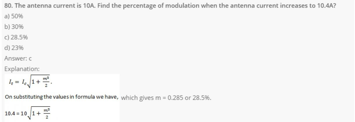
81. Find the total power, if the carrier of an AM transmitter is 800W and it is modulated to 50%?
a) 100W
b) 800W
c) 500W
d) 900W
Answer: d
Explanation: PT=PC (1+u2⁄2), according to the problem PC = 800W and m = 0.5. On substituting values in the equation we get PT=800(1+ 0.52⁄2) = 900W.
82. Aliasing refers to ________
a) Sampling of signals less than at Nyquist rate
b) Sampling of signals at Nyquist rate
c) Sampling of signals greater than at Nyquist rate
d) Unsampled the original signal
Answer: a
Explanation: Aliasing refers to the sampling of signals less than at Nyquist rate. Nyquist rate states that the rate of sampling of signals should be greater than or equal to twice the bandwidth of modulating signal. It gets reduced if sampling is done at a higher rate than nyquist rate of sampling. Aliasing can be avoided by using anti-aliasing filters.
1. Find the Nyquist rate and Nyquist interval of sin(2πt).
a) 2 Hz, 12 sec
b) 12 Hz, 12 sec
c) 12 Hz, 2 sec
d) 2 Hz, 2 sec
Answer: a
Explanation: We know that sin ω0 t ↔ jπ[δ(ω+ω0) – δ(ω-ω0)]
sin 2πt ↔ jπ[δ(ω+2π)-δ(ω-2π)]
Here ωm = 2π
But ωm = 2πfm
∴ fm = 1 Hz
Nyquist rate, Fs = 2fm = 2 Hz
Nyquist interval, T = 12fm=12sec.
2. Find the Nyquist rate and Nyquist interval of sinc[t].
a) 1 Hz, 1 sec
b) 2 Hz, 2 sec
c) 12 Hz, 2 sec
d) 2 Hz, 12sec
Answer: a
Explanation: We know that sinc[t] ↔ G2π(ω)
Here ωm = 2π
2πfm = π
∴ 2fm = 1
Nyquist rate, Fs = 2fm = 1 Hz
Nyquist interval, T = 12fm = 1 sec.
3. Find the Nyquist rate and Nyquist interval of Asinc[t].
a) 2 Hz, 2 sec
b) 1 Hz, 1 sec
c) 12 Hz, 1 sec
d) 1 Hz, 12 sec
Answer: b
Explanation: Nyquist rate and Nyquist interval are independent of Amplitude (magnitude scaling). But time scaling will change the rate.
We know that sinc[t] ↔ G2π(ω)
Here ωm = 2π
2πfm = π
∴ 2fm = 1
Nyquist rate, Fs = 2fm = 1 Hz
Nyquist interval, T = 12fm = 1 sec.
∴Fs = 1 Hz, T = 1 sec.
4. Find the Nyquist rate and Nyquist interval of sinc[200t].
a) 200 Hz, 1200 sec
b) 200 Hz, 200 sec
c) 1200 Hz, 200 sec
d) 100 Hz, 100 sec
Answer: a
Explanation: Here ωm=200π
2πfm=200π
2fm=200 Hz
Nyquist rate, Fs = 2fm = 200 Hz
Nyquist interval, T = 12fm=1200 sec.
5. Which of the following is the process of ‘aliasing’?
a) Peaks overlapping
b) Phase overlapping
c) Amplitude overlapping
d) Spectral overlapping
Answer: d
Explanation: Aliasing is defined as the phenomenon in which a high frequency component in the frequency spectrum of the signal takes the identity of a lower frequency component in the spectrum of the sampled signal.
Aliasing can occur if either of the following condition exists:
• The signal is not band-limited to a finite range.
• The sampling rate is too low.
6. Find the Nyquist rate and Nyquist interval for the signal f(t)=sin500πtπt.
a) 500 Hz, 2 sec
b) 500 Hz, 2 msec
c) 2 Hz, 500 sec
d) 2 Hz, 500 msec
Answer: b
Explanation: Given f(t) = sin500πtπt
Frequency, ωm = 500π
2πfm = 500π
2fm = 500 Hz
Nyquist rate, Fs = 2fm = 500 Hz
Nyquist interval, T = 12fm=1500 = 2 msec.
7. Find the Nyquist rate and Nyquist interval for the signal f(t) = [sin500πtπt]2.
a) 1000 Hz, 1 msec
b) 1 Hz, 1000 sec
c) 1000 Hz, 1 sec
d) 1000 Hz, 1000 sec
Answer: a
Explanation: Given f(t) = [sin500πtπt]2=1−cos1000πt(πt)2
Frequency, ωm = 1000π
2πfm = 1000π
2fm = 1000 Hz
Nyquist rate, Fs = 2fm = 1000 Hz
Nyquist interval, T = 12fm=11000 = 1 msec.
8. Find the Nyquist rate and Nyquist interval for the signal f(t) = 1 + sinc300πt.
a) 300 Hz, 3 msec
b) 300 Hz, 3.3 msec
c) 30 Hz, 3 msec
d) 3 Hz, 3 msec
Answer: b
Explanation: Given f(t) = 1 + sinc300πt
Frequency, ωm = 300π
2πfm = 300π
2fm = 300 Hz
Nyquist rate, Fs = 2fm = 300 Hz
Nyquist interval, T = 12fm=1300 = 3.3 msec.
9. Find the Nyquist rate and Nyquist interval for the signal f(t) = rect(200t).
a) ∞ Hz, 0 sec
b) 0 Hz, ∞ sec
c) ∞ Hz, ∞ Hz
d) 0 Hz, 0 sec
Answer: a
Explanation: Given f(t) = rect(200t), which is a rectangular pulse signal having pulse width of 1/200 seconds. Since the signal is a finite duration signal, it is not band-limited. The signal spectrum consists of infinite frequencies.
Hence, Nyquist rate is infinity and Nyquist interval is zero.
10. The sampling frequency of a signal is Fs = 2000 samples per second. Find its Nyquist interval.
a) 0.5 sec
b) 5 msec
c) 5 sec
d) 0.5 msec
Answer: b
Explanation: Given Fs = 2000 samples per second
Nyquist interval, T = 1Fs=12000 = 0.5 msec.
11. Determine the Nyquist rate of the signal x(t) = 1 + cos 2000πt + sin 4000πt.
a) 2000 Hz
b) 4000 Hz
c) 1 Hz
d) 6000 Hz
Answer: b
Explanation: Given x(t) = 1 + cos 2000πt + sin 4000πt
Highest frequency component in 1 is zero
Highest frequency component in cos2000πt is ωm1 = 2000π
Highest frequency component in sin4000πt is ωm2 = 4000π
So the maximum frequency component in x(t) is ωm = 4000π [highest of 0, 2000π, 4000π]
∴ 2πfm = 4000π
2fm = 4000
Nyquist rate, Fs = 2fm = 4000 Hz.
12. Find the Nyquist rate and Nyquist interval for the signal f(t) = -10 sin 40πt cos 300πt.
a) 40 Hz, 40 sec
b) 340 Hz, 340 sec
c) 300 Hz, 300 sec
d) 340 Hz, 1340 sec
Answer: d
Explanation: sin 40πt has highest frequency ωm1 = 40π
cos300πt has highest frequency ωm2 = 300π
As we know, multiplication in time domain is equivalent to convolution in frequency domain, the convoluted spectra will have highest frequency component ωm = ωm1 + ωm2 = 40π + 300π
ωm = 340π
2πfm = 340π
2fm = 340
Nyquist rate, Fs = 2fm = 340 Hz
Nyquist interval, T = 1Fs=1340 sec.
13. What is the full form of SONET?
a) Synchronous Optical Network
b) Standard Optical Network
c) Secret Optical Network
d) Service Optical Network
Answer: a
Explanation: SONET stands for Synchronous Optical Network. SONET transfers multiple digital bit streams in a synchronized way over optical fiber using lasers.
14. VFO stands for ________
a) Voltage Feedback Oscillator
b) Variable Feedback Oscillator
c) Voltage Frequency Oscillator
d) Variable Frequency Oscillator
Answer: d
Explanation: VFO stands for Variable Frequency Oscillator. VFO is an oscillator whose frequency can be tuned over some range. It is a necessary component in any tunable radio. It is mostly used in superheterodyne receivers.
15. What is used in Hartley oscillator?
a) a piezoelectric crystal
b) two resistor divider
c) a two-capacitor divider
d) a tapped inductor
Answer: d
Explanation: In Hartley oscillator, the oscillation frequency is determined by a tuned circuit consisting of capacitors and inductors. Thus, it is an LC oscillator whose frequency can be varied. Hartley oscillator was invented in 1915.
16. The conditions for sinusoidal oscillation from an amplifier are called _________
a) Loop-gain criteria
b) Hartley criteria
c) Biasing criteria
d) Barkhausen criteria
Answer: d
Explanation: The conditions for sinusoidal oscillation from an amplifier are called Barkhausen criteria. It was invented in 1921.
17. Which parts of a sinusoidal carrier can be modulated?
a) only amplitude
b) only frequency
c) its amplitude, frequency and direction
d) its amplitude, frequency and phase angle
Answer: d
Explanation: If the carrier wave is sinusoidal, then we can vary its amplitude, frequency, and phase in proportion with the wave which is transmitted.
18. The power density of a flicker noise is _________
a) low at high frequencies
b) greater at low frequencies
c) greater at high frequencies
d) low at low frequencies
Answer: b
Explanation: Flicker noise is a form of noise that exhibits an inverse frequency power density curve. It usually occurs at low frequencies. Its power density is greater at low frequencies.
19. Power above the minimum required by an optical receiver is called ________
a) phase margin
b) system margin
c) excess gain
d) gain margin
Answer: b
Explanation: System margin is the term used when the applied power is above the minimum required power by an optical receiver.
20. What is the full form of DWDM?
a) Dense Wavelength Division Multiplexing
b) Dense Wavelength Division Modulation
c) Directed Wavelength Division Multiplexing
d) Directed Wavelength Division Modulation
Answer: a
Explanation: DWDM stands for Dense Wavelength Division Multiplexing. In DWDM, each signal has its own separated wavelength.
21. FTTC stands for ________
a) Fiber To The Curb
b) Fiber Telephone Transmission Cable
c) Fiber Transmission Timing Cable
d) Fiber Telephone Timing Cable
Answer: a
Explanation: FTTC stands for Fiber To The Curb. It is a replacement of Plain Old Telephone Service (POTS) that we see in our neighborhood.
22. The process of using a pulse signal to represent information is called _______
a) Pulse modulation
b) Frequency modulation
c) Amplitude modulation
d) Phase modulation
Answer: a
Explanation: In pulse modulation, the information to be transmitted is represented by a series of binary pulses. Since the pulse information is binary in nature analog signal shave to be converted to digital before transmitting.
23. Which of the following is false with respect to pulse modulation?
a) Less power consumption
b) Low noise
c) Degraded signal can be regenerated
d) Can transmit analog as well as digital waves
Answer: d
Explanation: Analog values cannot be transmitted as such by pulse modulation since it can only transmit binary data. However, the analog signal can be converted into digital using an ADC and then transmitted via pulse modulation.
24. Which of the following is not a form of pulse modulation?
a) Pulse amplitude modulation
b) Pulse width modulation
c) Pulse position modulation
d) Pulse frequency modulation
Answer: d
Explanation: There are four basic forms of pulse modulation. They are: pulse amplitude modulation, pulse width modulation, pulse position modulation pulse code modulation. In any form of pulse modulation, the frequency of the signal is not changed.
25. How many voltage levels are present in a PWM signal?
a) 0
b) 1
c) 2
d) 3
Answer: c
Explanation: The amplitude of PWM is binary in nature meaning that it has only two levels. The amplitude of the modulating signals varies the width of the pulses generated.
26. Power consumption is low in pulse modulation.
a) True
b) False
Answer: a
Explanation: In pulse modulation, the carrier is not transmitted continuously but in pulses whose width is determined by the amplitude of the modulating signal. The duty cycle is made in such a way that the carrier is off for a longer time than it bursts hence the average power consumption is low.
27. Which pulse modulation technique is least expensive?
a) Pulse amplitude modulation
b) Pulse width modulation
c) Pulse position modulation
d) Pulse code modulation
Answer: a
Explanation: Out of all the pulse modulation techniques, Pulse amplitude modulation is the least expensive and simplest to implement. In pulse amplitude modulation, the amplitude of the pulse varies with the amplitude of the modulating signal.
28. Which of the following is false with respect to pulse position modulation?
a) Can be transmitted in broadband
b) Modulates a high frequency carrier
c) Pulse is narrow
d) Pulse width changes in accordance with the amplitude of modulating signal
Answer: d
Explanation: In PPM, the pulses change position according to the amplitude of the analog signal. The pulses are very narrow. These pulse signals may be transmitted in a baseband form, but in most applications, they modulate a high-frequency radio carrier.
29. Pulse modulation is not used in which of the following?
a) Telemetry systems
b) Remote control models
c) Switch power modes
d) Communication of airplane with ATC
Answer: d
Explanation: Pulse modulation is used in telemetry systems to monitor spacecraft or missile, RC models, for switching power supplies like regulators and also as audio switching power amplifiers. Communication of airplane with ATC is amplitude modulated waves.
30. The process of signal compression and expansion used to reduce distortion and noise is called _____
a) Amplification
b) Companding
c) Compressing
d) Modulating
Answer: b
Explanation: To reduce the effects of noise and distortion in pulse modulation, a process called companding is done. Companding is a process of signal compression and expansion.
31. What type of digital modulation is widely used for digital data transmission?
a) Pulse amplitude modulation
b) Pulse width modulation
c) Pulse position modulation
d) Pulse code modulation
Answer: d
Explanation: The most widely used technique for digitizing information signals for electronic data transmission is pulse code modulation. It has uniform transmission quality and also can be used when the signal traffic is high.
32. What is the output voltage if the input voltage of a compander with a maximum voltage range of 1 V and a μ of 255 is 0.25?
a) 0V
b) 0.25V
c) 0.5V
d) 0.75V
Answer:d
Explanation: ![]()
33. What is the output voltage if the input voltage of a compander with a maximum voltage range of 1 V and a μ of 255 is 0.8V0?
a) 0.08V
b) 0.458V
c) 1.02V
d) 1.54V
Answer: c
Explanation: 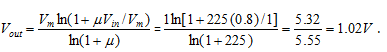
34. The signals which are obtained by encoding each quantized signal into a digital word is called as
a) PAM signal
b) PCM signal
c) FM signal
d) Sampling and quantization
Answer: b
Explanation: Pulse code modulation is the name for the class of signals which are obtained by encoding the quantized signals into a digital word.
35. The length of the code-word obtained by encoding quantized sample is equal to
a) l=log(to the base 2)L
b) l=log(to the base 10)L
c) l=2log(to the base 2)L
d) l=log(to the base 2)L/2
Answer: a
Explanation: The quantized sample which are digitally encoded into l bit value code-word. The length l can be calculated as l=log(to the base 2)L.
36. Quantization noise can be reduced by ________ the number of levels.
a) Decreasing
b) Increasing
c) Doubling
d) Squaring
Answer: b
Explanation: The process of quantization replaces the true signal with the approximation(quantization noise). By increasing the number of quantization level the quantization noise can be reduced.
37. In PCM encoding, quantization level varies as a function of ________
a) Frequency
b) Amplitude
c) Square of frequency
d) Square of amplitude
Answer: b
Explanation: In linear PCM the quantization levels are uniform. But in normal PCM encoding the quantization level vary according to the amplitude, based of A-law of Myu-law.
38. What is bit depth?
a) Number of quantization level
b) Interval between two quantization levels
c) Number of possible digital values to represent each sample
d) None of the mentioned
Answer: c
Explanation: One of the properties of PCM signal which determines its stream fidelity is bit depth which is the number of possible digital values that can be used to represent each sample.
39. Choosing a discrete value that is near but not exactly at the analog signal level leads to
a) PCM error
b) Quantization error
c) PAM error
d) Sampling error
Answer: b
Explanation: One of the limitations of PCM is quantization error which occurs when we choose a discrete value at some near by value and not at the analog signal level.
40. In PCM the samples are dependent on ________
a) Time
b) Frequency
c) Quanization leavel
d) Interval between quantization level
Answer: a
Explanation: The samples depend on time,an accurate clock is required for accurate reproduction.
41. DPCM encodes the PCM values based on
a) Quantization level
b) Difference between the current and predicted value
c) Interval between levels
d) None of the mentioned
Answer: b
Explanation: Differential PCM encodes the PCM value based on the difference between the previous sample and the present sample value.
42. Delta modulation uses _____ bits per sample.
a) One
b) Two
c) Four
d) Eight
Answer: a
Explanation: Delta modulation is used for analog to digital conversion and vice versa. It is a simple form of DPCM. Its uses 1 bit per sample. It also depends on the difference between the current and previous sample values.
43. Sample resolution for LPCM ____ bits per sample.
a) 8
b) 16
c) 24
d) All of the mentioned
Answer: d
Explanation: Common sampling resolution for LPCM are 8, 16, 20, 24 bits per sample.
44. Adaptive DPCM is used to
a) Increase bandwidth
b) Decrease bandwidth
c) Increase SNR
d) None of the mentioned
Answer: b
Explanation: Adaptive DPCM is used to decrease required bandwidth for the given SNR.
45. Flat top sampling of low pass signals
a) Gives rise to aperture effect
b) Implies over sampling
c) Leads to aliasing
d) Introduces delay distortion
Answer: a
Explanation: Flat top sampling of low pass signals gives rise to aperture effect.
46. In a delta modulation system, granular noise occurs when the
a) Modulating signal increases rapidly
b) Pulse rate decreases
c) Pulse amplitude decreases
d) Modulating signal remains constant
Answer: d
Explanation: In a delta modulation system, granular noise occurs when the modulating signal remains constant.
47. A PAM signal can be detected using
a) Low pass filter
b) High pass filter
c) Band pass filter
d) All pass filter
Answer: a
Explanation: A PAM signal can be detected by using low pass filter.
48. Coherent demodulation of FSK signal can be performed using
a) Matched filter
b) BPF and envelope detectors
c) Discriminator
d) None of the mentioned
Answer: a
Explanation: Coherent demodulation of FSK signal can be performed using matched filter.
49. The use of non uniform quantization leads to
a) Reduction in transmission bandwidth
b) Increase in maximum SNR
c) Increase in SNR for low level signals
d) Simplification of quantization process
Answer: c
Explanation: The use of non uniform quantization leads to increase in SNR for low level signals.
50. Which of the following requires a synchronizing signal?
a) Single channel PPM system
b) PAM
c) DM
d) All of the mentioned
Answer: b
Explanation: PAM requires a synchronizing signal.
51. A PWM signal can be generated by
a) An astable multi vibrator
b) A monostable multi vibrator
c) Integrating a PPM signal
d) Differentiating a PPM signal
Answer: b
Explanation: A PWM signal can be generated by a mono stable multi vibrator.
52. TDM is less immune to cross-talk in channel than FDM.
a) True
b) False
Answer: b
Explanation: False because different message signals are not applied to the channel simultaneously.
53. In an ideal TDM system, the cross correlation between two users of the system is
a) 1
b) 0
c) Infinity
d) -1
Answer: b
Explanation: In an ideal TDM system, the cross correlation between two users of the system is 0.
54. TDM requires
a) Constant data transmission
b) Transmission of data samples
c) Transmission of data at random
d) Transmission of data of only one measured
Answer: b
Explanation: TDM requires transmission of data samples.
55. Which is based on orthogonality?
a) TDM
b) FDM
c) TDM & FDM
d) None of the mentioned
Answer: b
Explanation: FDM technique is based on the orthogonality of sinusoids.
56. Which provides constant delay?
a) Synchronous TDM
b) Non synchronous TDM
c) Synchronous & Non synchronous TDM
d) None of the mentioned
Answer: a
Explanation: Synchronous time division multiplexing provides constant bandwidth and constant delay.
57. Random access is
a) Distributed
b) Fault tolerant
c) Distributed & Fault tolerant
d) None of the mentioned
Answer: c
Explanation: Random access is simple, distributed and very fault tolerant.
58. Example of reservation system is
a) Synchronous TDM
b) Non synchronous TDM
c) Synchronous & Non synchronous TDM
d) None of the mentioned
Answer: a
Explanation: Synchronous TDM is an example for the reservation system.
59. Reservation systems are useful when
a) Delay is small
b) Delay is large
c) Delay is small or large
d) None of the mentioned
Answer: b
Explanation: Reservation systems are useful when delays are large.
60. In slotted system, access is
a) Synchronous
b) Asynchronous
c) Synchronous & Asynchronous
d) None of the mentioned
Answer: b
Explanation: In slotted system, access is asynchronous and requires addressing information inside.
61. In CSMA, collision window is _____ to cable length.
a) Equal
b) Greater
c) Lesser
d) None of the mentioned
Answer: b
Explanation: The collision window is twice the cable length.
62. Which isolates collision?
a) Bridges
b) Routers
c) Bridges & Routers
d) None of the mentioned
Answer: c
Explanation: Bridges and routers isolates collision.
63. Minimum packet size increases as
a) Speed increases
b) Distance increases
c) Speed & Distance increases
d) None of the mentioned
Answer: c
Explanation: As speed and distance goes up, minimum packet size also goes up.
64. Which are non orthogonal multiplexing?
a) TDM
b) FDM
c) TDM & FDM
d) None of the mentioned
Answer: d
Explanation: TDM and FDM are both orthogonal multiplexing.
1. Self information should be
a) Positive
b) Negative
c) Positive & Negative
d) None of the mentioned
Answer: a
Explanation: Self information is always non negative.
2. The unit of average mutual information is
a) Bits
b) Bytes
c) Bits per symbol
d) Bytes per symbol
Answer: a
Explanation: The unit of average mutual information is bits.
3. When probability of error during transmission is 0.5, it indicates that
a) Channel is very noisy
b) No information is received
c) Channel is very noisy & No information is received
d) None of the mentioned
Answer: c
Explanation: When probability of error during transmission is 0.5 then the channel is very noisy and thus no information is received.
4. Binary Huffman coding is a
a) Prefix condition code
b) Suffix condition code
c) Prefix & Suffix condition code
d) None of the mentioned
Answer: a
Explanation: Binary Huffman coding is a prefix condition code.
5. The event with minimum probability has least number of bits.
a) True
b) False
Answer: b
Explanation: In binary Huffman coding the event with maximum probability has least number of bits.
6. The method of converting a word to stream of bits is called as
a) Binary coding
b) Source coding
c) Bit coding
d) Cipher coding
Answer: b
Explanation: Source coding is the method of converting a word to stream of bits that is 0’s and 1’s.
7. When the base of the logarithm is 2, then the unit of measure of information is
a) Bits
b) Bytes
c) Nats
d) None of the mentioned
Answer: a
Explanation: When the base of the logarithm is 2 then the unit of measure of information is bits.
8. When X and Y are statistically independent, then I (x,y) is
a) 1
b) 0
c) Ln 2
d) Cannot be determined
Answer: b
Explanation: When X and Y are statistically independent the measure of information I (x,y) is 0.
9. The self information of random variable is
a) 0
b) 1
c) Infinite
d) Cannot be determined
Answer: c
Explanation: The self information of a random variable is infinity.
10. Entropy of a random variable is
a) 0
b) 1
c) Infinite
d) Cannot be determined
Answer: c
Explanation: Entropy of a random variable is also infinity.
11. Which is more efficient method?
a) Encoding each symbol of a block
b) Encoding block of symbols
c) Encoding each symbol of a block & Encoding block of symbols
d) None of the mentioned
Answer: b
Explanation: Encoding block of symbols is more efficient than encoding each symbol of a block.
12. Lempel-Ziv algorithm is
a) Variable to fixed length algorithm
b) Fixed to variable length algorithm
c) Fixed to fixed length algorithm
d) Variable to variable length algorithm
Answer: a
Explanation: Lempel-Ziv algorithm is a variable to fixed length algorithm.
13. Coded system are inherently capable of better transmission efficiency than the uncoded system.
a) True
b) False
Answer: a
Explanation: Yes, the coded systems are capable of better transmission efficiency than the uncoded system.
14. The minimum nyquist bandwidth needed for baseband transmission of Rs symbols per second is
a) Rs
b) 2Rs
c) Rs/2
d) Rs2
Answer: c
Explanation: Theoretical minimum nyquist bandwidth needed for the baseband transmission of Rs symbols per second without ISI is Rs/2.
15. The capacity relationship is given by
a) C = W log2 ( 1+S/N )
b) C = 2W log2 ( 1+S/N )
c) C = W log2 ( 1-S/N )
d) C = W log10 ( 1+S/N )
Answer: a
Explanation: The capacity relationship from Shannon-hartley capacity theorem is given by C = W log2 ( 1+S/N ).
16. Which parameter is called as Shannon limit?
a) PB/N0
b) EB/N0
c) EBN0
d) None of the mentioned
Answer: b
Explanation: There exists a limiting value for EB/N0 below which they can be no error free communication at any information rate. This EB/N0 is called as Shannon limit.
17. Entropy is the measure of
a) Amount of information at the output
b) Amount of information that can be transmitted
c) Number of error bits from total number of bits
d) None of the mentioned
Answer: a
Explanation: Entropy is defined as the average amount of information per source output.
18. Equivocation is the
a) Conditional entropy
b) Joint entropy
c) Individual entropy
d) None of the mentioned
Answer: a
Explanation: Shannon uses a correction factor called equivocation to account for uncertainty in the received signal. It is defined as the conditional entropy of the message X given Y.
19. For a error free channel, conditional probability should be
a) Zero
b) One
c) Equal to joint probability
d) Equal to individual probability
Answer: a
Explanation: For a error free channel conditional probability should be zero, because having received Y there is complete certainty about the message X.
20. Average effective information is obtained by
a) Subtracting equivocation from entropy
b) Adding equivocation with entropy
c) Ratio of number of error bits by total number of bits
d) None of the mentioned
Answer: a
Explanation: According to Shannon the average effective information is obtained by subtracting the equivocation from the entropy of the source.
21. Turbo codes are
a) Forward error correction codes
b) Backward error correction codes
c) Error detection codes
d) None of the mentioned
Answer: a
Explanation: Turbo codes are a class of high performance forward error correction codes.
22. Components used for generation of turbo codes are
a) Inter leavers
b) Punching pattern
c) Inter leavers & Punching pattern
d) None of the mentioned
Answer: c
Explanation: There are many instances of turbo codes, using different component encoders, input/output ratios, inter leavers, punching patterns.
23. Decoders are connected in series.
a) True
b) False
Answer: a
Explanation: Two elementary decoders are connected in serial connection for decoding the turbo codes.
24. The inter leaver connected between the two decoders is used to
a) Remove error bursts
b) Scatter error bursts
c) Add error bursts
d) None of the mentioned
Answer: b
Explanation: An inter leaver installed between the two decoders connected in series is used to scatter error bursts.
25. In soft decision approach what does -127 mean?
a) Certainly one
b) Certainly zero
c) Very likely zero
d) Very likely one
Answer: b
Explanation: The decoder front end produces an integer for each bit in the data stream. This integer is the measure of how likely it is that the bit 0 or 1 and is called as soft bit. It ranges from -127 to 127. Here -127 represents certainly zero.
26. In soft decision approach 100 means?
a) Certainly one
b) Certainly zero
c) Very likely zero
d) Very likely one
Answer: d
Explanation: The decoder front end produces an integer for each bit in the data stream. This integer is the measure of how likely it is that the bit 0 or 1 and is called as soft bit. It ranges from -127 to 127. Here 100 represents very likely one.
27. In soft decision approach 0 represents
a) Certainly one
b) Certainly zero
c) Very likely zero
d) Could be either zero or one
Answer: d
Explanation: The decoder front end produces an integer for each bit in the data stream. This integer is the measure of how likely it is that the bit 0 or 1 and is called as soft bit. It ranges from -127 to 127. Here 0 represents ‘could be either zero or one’.
Prepare For Your Placements: https://lastmomenttuitions.com/courses/placement-preparation/
![]()
/ Youtube Channel: https://www.youtube.com/channel/UCGFNZxMqKLsqWERX_N2f08Q
Follow For Latest Updates, Study Tips & More Content!
Not a member yet? Register now
Are you a member? Login now