Get Latest Exam Updates, Free Study materials and Tips

1. A solid copper sphere, 10 cm in diameter is deprived of 1020 electrons by a charging scheme. The charge on the sphere is _________
a) 160.2 C
b) -160.2 C
c) 16.02 C
d) -16.02 C
Answer: c
Explanation: n 1020, Q = ne = e 1020 = 16.02 C.
Charge on sphere will be positive.
2. A lightning bolt carrying 15,000 A lasts for 100 s. If the lightning strikes an airplane flying at 2 km, the charge deposited on the plane is _________
a) 13.33 C
b) 75 C
c) 1500 C
d) 1.5 C
Answer: d
Explanation: dQ = i dt = 15000 x 100µ = 1.5 C.
3. If 120 C of charge passes through an electric conductor in 60 sec, the current in the conductor is _________
a) 0.5 A
b) 2 A
c) 3.33 mA
d) 0.3 mA
Answer: b
Explanation: i = dQ/dt = 120/60 = 2A.
4. The energy required to move 120 coulomb through 3 V is _________
a) 25 mJ
b) 360 J
c) 40 J
d) 2.78 mJ
Answer: b
Explanation: W = Qv = 360 J.
5. Consider the circuit graph shown in figure below. Each branch of circuit graph represent a circuit element. The value of voltage V1 is:
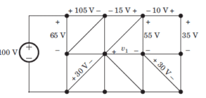
a) 30 V
b) 25 V
c) 20 V
d) 15 V
Answer: d
Explanation: 100 = 65 + V2 => V2 = 35 V
V3 – 30 = V2 => V3 = 65 V
105 – V3 + V4 – 65 = 0 => V4 = 25 V
V4 + 15 – 55 + V1 = 0 => V1 = 15 V.
6. What will be the value of Req in the following Circuit?
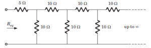
a) 11.86 ohm
b) 10 ohm
c) 25 ohm
d) 11.18 ohm
Answer: d
Explanation:
We infer from the given diagram that the same pattern is followed after every 10ohm resistor. The infinite pattern in parallel as a whole is considered as to be Rx.
Thus, Rx = R + (R||Rx)
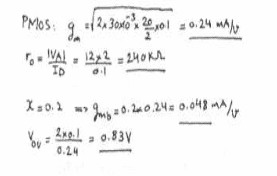
Solving for Rx, we get Rx = 1.62R, where R=10ohm.
So we have Rx = (1.62ohm)*(10ohm), which gives Rx=16.2ohm
Therefore, Req = 5 + (10||16.2)
=> 5 + [(10*16.2)/(10+16.2)] => Req = 5 + (162/26.2) which gives Req=11.18 ohm.
7. In the circuit the dependent source __________
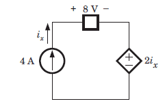
a) supplies 16 W
b) absorbs 16 W
c) supplies 32 W
d) absorbs 32 W
Answer: d
Explanation: P = VIx = 2Ix Ix = 2 x 16 or 32 watt (absorb).
8. Twelve 6 ohm resistors are used to form an edge of a cube. The resistance between two diagonally opposite corner of the cube (in ohm) is ________
a) 5/6
b) 6/5
c) 5
d) 6
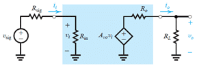
Answer: c
Explanation:
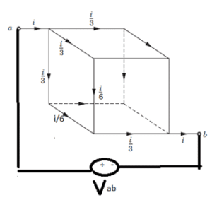
The current I will be distributed to the cube branches symmetrically.
Connecting a voltage source Vab across the terminals and applying kvl in the outer loop, we have
=> -Vab + (i/3+i/6+i/3)*R = 0 (where R is given as 6ohm)
=> Vab = 5i
=> Req=Vab/i, which gives Req = 5ohm.
9. The energy required to charge a 10 µF capacitor to 100 V is ________
a) 0.1 J
b) 0.05 J
c) 5 x 10(-9) J
d) 10 x 10(-9) J
Answer: b
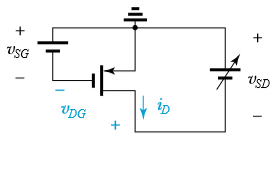
Explanation: Energy provided is equal to 0.5 CVxV.
10. A capacitor is charged by a constant current of 2 mA and results in a voltage increase of 12 V in a 10 sec interval. The value of capacitance is ________
a) 0.75 mF
b) 1.33 mF
c) 0.6 mF
d) 1.67 mF
Answer: d
Explanation: The capacitor current is given as i=C*(dv/dt), where dv/dt is the derivative of voltage, dt=t2-t1 given as 10 sec and dv is the change in voltage which is given as 12V.
So, we have C=i/(dv/dt)
=> C = 2mA/(12/10) = 2mA/(1.2).
Hence C = 1.67mF.
11. How many junction/s do a diode consist?
a) 0
b) 1
c) 2
d) 3
Answer: b
Explanation: Diode is a one junction semiconductor device which has one cathode and anode. The junction is of p-n type.
12. If the positive terminal of the battery is connected to the anode of the diode, then it is known as
a) Forward biased
b) Reverse biased
c) Equilibrium
d) Schottky barrier
Answer: a
Explanation: When a positive terminal is connected to the anode, the diode is forward biased which lets the flow of the current in the circuit.
13. During reverse bias, a small current develops known as
a) Forward current
b) Reverse current
c) Reverse saturation current
d) Active current
Answer: c
Explanation: When the diode is reverse biased, a small current flows between the p-n junction which is of the order of the Pico ampere. This current is known as reverse saturation current.
14. If the voltage of the potential barrier is V0. A voltage V is applied to the input, at what moment will the barrier disappear?
a) V< V0
b) V= V0
c) V> V0
d) V<< V0
Answer: b
Explanation: When the voltage will be same that of the potential barrier, the potential barrier disappears resulting in flow of current.
15. During the reverse biased of the diode, the back resistance decrease with the increase of the temperature. Is it true or false?
a) True
b) False
Answer: a
Explanation: Due to the increase in the reverse saturation current due to the increase in the temperature, the back resistance decrease with the increasing temperature.
16. What is the maximum electric field when Vbi=2V , VR=5V and width of the semiconductor is 7cm?
a) -100V/m
b) -200V/m
c) 100V/m
d) 200V/m
Answer: b
Explanation: Emax=-2(Vbi+VR)/W
=-2(2+5)/ (7*10-2)
=-200V/m.
17. When the diode is reverse biased with a voltage of 6V and Vbi=0.63V. Calculate the total potential.
a) 6V
b) 6.63V
c) 5.27V
d) 0.63V
Answer: b
Explanation: Vt=Vbi+VR
=0.63+6
=6V.
18. It is possible to measure the voltage across the potential barrier through a voltmeter?
a) True
b) False
Answer: b
Explanation: The contacts of the voltmeter have some resistance which will not accurately measure the voltage across the potential barrier. Thus, it is not possible to measure the voltage across the potential barrier.
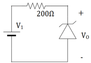
19. What will be the output of the following circuit? (Assume 0.7V drop across the diode)
a) 12V
b) 12.7V
c) 11.3V
d) 0V
Answer: c
Explanation: V=12-0.7
=11.3V.
20. Which of the following formula represents the correct formula for width of the depletion region?
Answer: a
Explanation: Option a is the correct formula.
21. When a forward biased is applied to a diode, the electrons enter to which region of the diode?
a) P-region
b) N-region
c) P-n junction
d) Metal side
Answer: a
Explanation: When the forward biased is applied, the electrons enter to the p-region and the holes enter to the n-region so that holes can flow from p-region to n-region. Whereas, the electrons can travel from n-region to p-region.
22. The number of injected minority carriers falls off linearly with the increase in the distance from the junction. Is it true or false?
a) True
b) False
Answer: b
Explanation: The number of minority carriers fall off exponentially rather than linearly with the increase in the distance from the junction.
23. What is the total current in a diode when x=0?
a) I = Ipn (0) – Inp (0)
b) I = Ipn (0) + Inp (0)
c) I = -Ipn (0) – Inp (0)
d) I = -Ipn (0) + Inp (0)
Answer: b
Explanation: At junction, the total current is equal to the minority hole current plus the minority electron current.
24. The current in the diode is
1. Unipolar
2. Bipolar
a) I only
b) II only
c) I and II both
d) Neither I nor II
Answer: b
Explanation: The current in the diode consists of both the electrons and holes. So, it is bipolar.
25. The current is constant throughout the device. Is it true or false?
a) True
b) False
Answer: a
Explanation: The current in the device is constant but the proportion due to the electrons and holes varies with distance.
26. Which of the following statements is correct under forward biased p-n diode?
a) current enters n side as hole current and leaves p side as electron current
b) current enters n side as electron current and leaves p side as hole current
c) current enters p side as hole current and leaves n side as electron current
d) current enters p side as hole current and leaves p side as electron current
Answer: c
Explanation: When the current flows in a p-n diode, the current enters p side as hole current and leaves n side as electron current.
27. Calculate the total current when Ipn (0)=1mA and Inp (0)=2mA.
a) 1mA
b) -1mA
c) 0
d) 3mA
Answer: d
Explanation: I=Ipn (0)+Inp (0)
=1mA+2mA
=3mA.
28. What is the hole current in the p region of the diode?
a) Ipp (x)=I-Inp (x)
b) Ipp (x)=I+Inp (x)
c) Ipp (x)=-I-Inp (x)
d) Ipp (x)=-I+Inp (x)
Answer: a
Explanation: The hole current in the p region is equal to the total current minus the minority electrons in the p region.
29. What does Inp represent?
a) Hole current in n region
b) Hole current in p region
c) Electron current in n region
d) Electron current in p region
Answer: d
Explanation: Inp constitutes of the electron current in the p region. It is the minority electron carrier in the p region.
30. Deep into the p side the current is a drift current Ipp of holes sustained by the small electric field in the semiconductor. Is the statement true or false?
a) True
b) False
Answer: a
Explanation: In the p region, the drift current is sustained into the p region by the small electric field which is formed at the junction in the semiconductor. So, the above statement is true.
31. The static resistance R of the diode is given by __________
a) V/I
b) V*I
c) V+I
d) V-I
Answer: a
Explanation: According to Ohms law the electric current in the circuit is directly proportion to voltage and inversely proportional to resistance so, R=V/I.
32. In the volt ampere characteristics of the diode, the slope of the line joining the operating point to the origin at any point is equal to reciprocal of the _________
a) resistance
b) conductance
c) voltage
d) current
Answer: a
Explanation: In the diode’s volt ampere characteristics, the line joining the operating point and the origin, at any point of the line is equal to the conductance so, it is reciprocal of the resistance.
33. At room temperature (VT = 26) what will be the approximate value of r when n=1 and I=100mA?
a) 26 ohms
b) 2.6 ohms
c) 260 ohms
d) 2600 ohms
Answer: c
Explanation: We know that R= (n*VT) /I, by substituting the value of n, VT, I we get R= 260 ohms, (1*26)/100*10-3 = 260 ohms.
34. In the diode volt ampere characteristics what will be the resistance if a slope is drawn between the voltages 50 to 100 and corresponding current 5 to 10?
a) 5 ohms
b) 10 ohms
c) 50 ohms
d) 100 ohms
Answer: b
Explanation: We know that, in volt ampere characteristics the resistance is equal to the reciprocal of the line joining the origin and operating point, R = dV/dI, by substituting the value of dV and dI we get R= 10ohms.
35. In piecewise linear characteristics what will be the RF value if the slope is 0.5?
a) 25 m ohms
b) 50 m ohms
c) 2 ohms
d) 10 ohms
Answer: c
Explanation: In piecewise linear characteristics the forward resistance will be equal to reciprocal of the slope so, RF = 1/slope, RF = 1/0.5 which is equal to 2 ohms.
36. A diode will behave as an open circuit if the voltage in the circuit is less than __________
a) cut off voltage
b) saturation voltage
c) leakage voltage
d) threshold voltage
Answer: d
Explanation: The diode made up of semiconductor has a certain threshold voltage only after which it behave as closed circuit in the sense it performs some operation if the threshold voltage is greater than the voltage in circuit.
37. What will be the approximate value of thermal voltage of diode?
a) 25mV at 300K
b) 30mV at 180K
c) 25mV at 180K
d) 30mV at 300K
Answer: a
Explanation: We know that the thermal voltage of diode is approximately equal to room temperature which is 300K then for all practical purpose the thermal voltage of diode is taken as 25mV so it will be 25mV at 300K.
38. What will be the thermal voltage of the diode if the temperature is 300K?
a) 25.8 mV
b) 50 mV
c) 50V
d) 19.627 mV
Answer: a
Explanation: The thermal voltage of the diode is given by, VT = KT/q, by substituting the values of T, K which is Boltzmann constant and q which is the charge of the electron we get VT = (300*1.38*10-23)/ (1.602*10-19), VT= 25.8mV.
39. What will be the diode resistance if the current in the circuit is zero?
a) 0 ohms
b) 0.7 ohms
c) 0.3 ohms
d) 1 ohms
Answer: a
Explanation: When the current in the circuit is zero there will be no flow of charges to resist hence the diode resistance will be zero.
40. Which of these following is not a characteristic of an ideal diode?
a) Perfect conductor when forward bias
b) Zero voltage across it when forward bias
c) Perfect insulator when reverse bias
d) Zero current through it when forward bias
Answer: d
Explanation: The diode acts as an ideal diode when it is a perfect conductor and has zero voltage across it during forward bias, a perfect insulator and zero current through it during reverse bias.
41. The percentage voltage regulation (VL) is given by_________
a) (VNL-VL)/VNL*100
b) (VNL+VL)/VNL*100
c) (VNL-VL)/VL*100
d) (VNL+VL)/VL*100
Answer: a
Explanation: The change in the output voltage from no load to full load condition is called as voltage regulation, where VNL is the voltage at no load condition. It is used to maintain a nearly constant output voltage. If the regulation is high, the output voltage is stable.
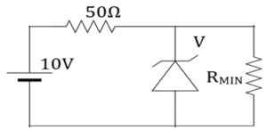
42. The limiting value of the current resistor used in a Zener diode (when used as a regulator)
a) (R)min=[(Vin)max + VZ/R
b) (R)min=[(Vin)max-VZ]/R
c) (R)min=[(Vin)max-VZ]R
d) (R)min=[(Vin)max+ VZ]R
Answer: b
Explanation: When the input voltage is maximum, the load current is minimum, the Zener current should not increase the maximum rated value. Therefore there should be a minimum value of resistor.
43. When the regulation by a Zener diode is with a varying input voltage, what happens to the voltage drop across the resistance?
a) Decreases
b) Has no effect on voltage
c) Increases
d) The variations depend on temperature
Answer: c
Explanation: When the input voltage varies, the input current also varies. This makes more current to flow in the diode. This increase in the current should balance a change in the load current. Hence the voltage drop increases across the resistor.
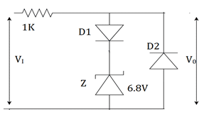
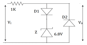
44. In the given limiter circuit, an input voltage Vi=10sin100πt is applied. Assume that the diode drop is 0.7V when it’s forward biased. The zener breakdown voltage is 6.8V.The maximum and minimum values of outputs voltage are _______
a) 6.1V,-0.7V
b) 0.7V,-7.5V
c) 7.5V,-0.7V
d) 7.5V,-7.5V
Answer: c
Explanation: With VI= 10V when maximum, D1 is forward biased, D2 is reverse biased. Zener is in breakdown region. VOMAX=sum of breakdown voltage and diode drop=6.8+0.7=7.5V. VOMIN=negative of voltage drop=-0.7V. There will be no breakdown voltage here.
45. Determine the maximum and minimum values of load current for which the Zener diode shunt regulator will maintain regulation when VIN=24V and R=500Ω. The Zener diode has a VZ=12V and (IZ)MAX=90mA.
a) 40mA, 0mA respectively
b) 36mA, 5mA respectively
c) 10mA, 6mA respectively
d) 21mA, 0mA respectively
Answer: d
Explanation: The current through the resistance R is given by, I=(VIN-VZ)/R= (24-12)/500=24mA. (IL)MAX=I-(IZ)MIN=24-3=21mA .This current is less than (IZ)MAX. So, we assume that all the input current flows through the Zener diode. Under this condition, (IL)MIN is 0mA.
46. Determine the minimum value of load resistance that can be used in the circuit with (IZ)Min=3mA. The input voltage is 10V and the resistance R is 500Ω. The Zener diode has a VZ=6V 0and (IZ)MAX=90mA.
a) 1KΩ
b) 2.4KΩ
c) 1.2KΩ
d) 3.6KΩ
Answer: c
Explanation: The I=(VIN-VZ)/R=(10-6)/500=8mA. (IL)MAX=I-(IZ)MIN=8-3=5mA. (RL)MIN=VZ/(IL)MAX=6/5m=1.2KΩ.
47. A Zener regulator has to handle supply voltage variation from 19.5V to 22.5V. Find the magnitude of regulating resistance, if the load resistance is 6KΩ. The Zener diode has the following specifications: breakdown voltage =18V, (IZ)Min=2µA, maximum power dissipation=60mW and Zener resistance =20Ω.
a) 0 < R < 500Ω
b) 77.8 < R < 500Ω
c) 77.8 < R < 100Ω
d) 18 < R < 500Ω
Answer: b
Explanation: (PZ)MAX/rZ=(IZ)MAX2 . So, (IZ)MAX =60m/20=54.8µA. IL=VO/RL=18/6000=3mA.
RMAX=(VMin-VZ)/[( IZ)Min+( IL)MAX]=(19.5-18)/(2µ+3m)=500Ω.
RMin=(VMAX-VZ)/[( IZ)MAX+( IL)Min]=(22.5-18)/(54.8m+3m)=77.8Ω.
48. A transistor series regulator has the following specifications: VIN=15V, VZ=8.3V, β=100, R=1.8KΩ, RL=2KΩ. What will be the Zener current in the regulator circuit?
a) 4.56mA
b) 3.26mA
c) 4.56mA
d) 3.68mA
Answer: d
Explanation: We know, VO=VZ-VBE=8.3-0.7=7.6V. VCE=VIN-V0=15-7.6=7.4V. So, IR=(VIN-VZ)/R=(15-8.3)/1.8m=3.72mA. IL=VO/RL=7.6/2000=3.8mA. IB=IL/ β=3.8mA/100=0.038mA. Finally, IZ=IR-IB=3.72-0.038=3.682mA.
49. When is a regulator used?
a) when there are small variations in load current and input voltage
b) when there are large variations in load current and input voltage
c) when there are no variations in load current and input voltage
d) when there are small variations in load current and large variations in input voltage
Answer: a
Explanation: The regulator has following limitations: 1.It has low efficiency for heavy load currents 2. The output voltage changes slightly due to Zener impedance. Hence, it is used when there are small variations in load current and input voltage.
50. A transistor in a series voltage regulator acts like a variable resistor. The value of its resistance is determined by _______
a) emitter current
b) base current
c) collector current
d) it is not controlled by the transistor terminals
Answer: b
Explanation: The principle is based on the fact that a large fraction of the increase in input voltage appears across the transistor so that the output voltage remains to be constant. When input voltage is increased, the output voltage also increases which biases the transistor towards less current.
51. A zener diode works on the principle of_________
a) tunneling of charge carriers across the junction
b) thermionic emission
c) diffusion of charge carriers across the junction
d) hopping of charge carriers across the junction
Answer: a
Explanation: Due to zener effect in reverse bias under high electric field strength, electron quantum tunneling occurs. It’s a mechanical effect in which a tunneling current occurs through a barrier. They usually cannot move through that barrier.
52. Which of the following are true about a zener diode?
1) it allows current flow in reverse direction also
2) it’s used as a shunt regulator
3) it operates in forward bias condition
a) 3 only
b) 1 and 2
c) 2 and 3
d) 2 only
Answer: b
Explanation: The operation of a zener diode is made in reverse bias when breakdown occurs. So, it allows currnt in reverse direction. The most important application of a zener diode is voltage or shunt regulator.
53. When the voltage across the zener diode increases_________
a) temperature remains constant and crystal ions vibrate with large amplitudes
b) temperature increases and crystal ions vibrate with large amplitudes
c) temperature remains constant and crystal ions vibrate with smaller amplitudes
d) temperature decreases and crystal ions vibrate with large amplitudes
Answer: b
Explanation: When voltage is increased, the tunnelling at reverse bias increases. The voltage rises temperature. The crystal ions with greater thermal energy tend to vibrate with larger amplitudes.
54. For the zener diode shown in the figure, the zener voltage at knee is 7V, the knee current is negligible and the zener dynamic resistance is 10Ω. If the input voltage (Vi) ranges from 10 to 16 volts, the output voltage (Vo) ranges from?
a) 7 to 7.29V
b) 6 to 7V
c) 7.14 to 7.43V
d) 7.2 to 8V
Answer: c
Explanation: If i is the current flowing, then V0=10i+7
i=(VI-7)/210. By substituting, if VI=10V then i=1/70 and V0=(1/7)+7=7.14V
if VI =16V then i=3/70 and V0=(3/7)+7=7.43V.
55. In the circuit below, the knee current of ideal zener diode is 10mA. To maintain 5V across the RL, the minimum value of RL is?
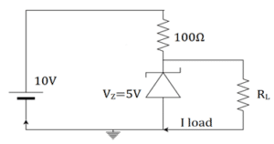
a) 120
b) 125
c) 250
d) 100
Answer: b
Explanation: Here, IKNEE=10mA, VZ=5V. I=IL+IZ. I= (10-5)/100=50mA
Now, 50=10+ILMAX .
ILMAX=40mA. RLMIN=5/40mA=125 Ω.
56. The zener diode in the circuit has a zener voltage of 5.8V and knee current of 0.5mA. The maximum load current drawn with proper function over input voltage range between 20 and 30V is?
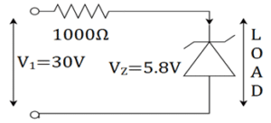
a) 23.7mA
b) 20mA
c) 26mA
d) 48.3mA
Answer: a
Explanation: Here, I1MAX=IZMIN+ILMAX.
IZMIN =0.5mA, I1MAX =(V1MAX-VZ )/RS . Putting the values we get , I1MAX =24.2mA.
So, 24.2-0.5=23.7mA.
57. In the given limiter circuit, an input voltage Vi=10sin100πt is applied. Assume that the diode drop is 0.7V when it’s forward biased. The zener breakdown voltage is 6.8V.The maximum and minimum values of outputs voltage are _______
a) 6.1V,-0.7V
b) 0.7V,-7.5V
c) 7.5V,-0.7V
d) 7.5V,-7.5V
Answer: c
Explanation: With VI= 10V when maximum, D1 is forward biased, D2 is reverse biased. Zener is in breakdown region. VOMAX=sum of breakdown voltage and diode drop=6.8+0.7=7.5V. VOMIN=negative of voltage drop=-0.7V. There will be no breakdown voltage here.
58. The 6V Zener diode shown has zener resistance and a knee current of 5mA. The minimum value of R so that the voltage does not drop below 6V is?
a) 1.2Ω
b) 80 Ω
c) 50 Ω
d) 70 Ω
Answer: b
Explanation: Here, Vz =6V, IZMIN=5mA.IS=IZMIN+ILMAX.
80=5+ILMAX . ILMAX=75Ma.RLMIN=VI/ILMAX=6/75mA
=80 Ω.
59. Avalanche breakdown in zener diode is ______
a) electric current multiplication takes place
b) phenomenon of voltage multiplication takes place
c) electrons are decelerated for a period of time
d) sudden rise in voltage takes place.
Answer: a
Explanation: The carriers in transition region are accelerated by electric field to energies. That energies are sufficient to create electron current multiplication. A single carrier that is energized will collide with another by gaining energy. Thus an avalanche multiplication takes place.
60. The zener diode is heavily doped because______
a) to have low breakdown voltage
b) to have high breakdown voltage
c) to have high current variations
d) to maintain perfect quiescent point
Answer: a
Explanation: The value of reverse breakdown voltage at which zener breakdown occurs is controlled by amount of doping. If the amount of doping is high, the value of voltage at which breakdown occurs will decrease. Better doping gives a sooner breakdown voltage.
1. The advantages over the vacuum triode for a junction transistor is_________
a) high power consumption
b) high efficiency
c) large size
d) less doping
Answer: b
Explanation: A junction transistor is an analogous to a vacuum triode. The main difference between them is that a transistor is a current device while a vacuum triode is a voltage device. The advantages of a transistor over a vacuum triode are long life, high efficiency, light weight, smaller in size, less power consumption.
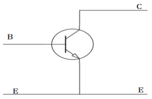
2. What is the left hand section of a junction transistor called?
a) base
b) collector
c) emitter
d) depletion region
Answer: c
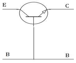
Explanation: The main function of this section is to supply majority charge carriers to the base. Hence it is more heavily doped in comparison to other regions. This forms the left hand section of the transistor.
3. In an NPN transistor, the arrow is pointed towards_________
a) the collector
b) the base
c) depends on the configuration
d) the emitter
Answer: d
Explanation: As regards to the symbols, the arrow head is always at the emitter. The direction indicates the conventional direction of current flow. In case of PNP transistor, it is from base to emitter.
4. Which of the following is true in construction of a transistor?
a) the collector dissipates lesser power
b) the emitter supplies minority carriers
c) the collector is made physically larger than the emitter region
d) the collector collects minority charge carriers
Answer: c
Explanation: In most of the transistors, the collector is made larger than emitter region. This is due to the fact that collector has to dissipate much greater power. The collector and emitter cannot be interchanged.
5. In the operation of an NPN transistor, the electrons cross which region?
a) emitter region
b) the region where there is high depletion
c) the region where there is low depletion
d) P type base region
Answer: d
Explanation: The electrons in the emitter region are repelled by the negative terminal of the battery towards the emitter junction. The potential barrier at the junction is reduced due to forward bias and base region is very thin and lightly doped, electrons cross the P type base region.
6. Which of the following are true for a PNP transistor?
a) the emitter current is less than the collector current
b) the collector current is less than the emitter current
c) the electrons are majority charge carriers
d) the holes are the minority charge carriers
Answer: b
Explanation: The 2 – 5% of holes is lost in recombination with electrons in the base region. The majority charge carriers are holes for a PNP transistor. Thus the collector current is slightly less than the emitter current.
7. In the saturated region, the transistor acts like a_________
a) poor transistor
b) amplifier
c) open switch
d) closed switch
Answer: d
Explanation: In saturated mode, both emitter and collector are forward biased. The negative of the battery is connected to emitter and similarly the positive terminals of batteries are connected to the base. The transistor now acts like a closed switch.
8. When does the transistor act like an open switch?
a) cut off region
b) inverted region
c) saturated region
d) active region
Answer: a
Explanation: In cut off region, both the junctions are reverse biased. The transistor has practically zero current because the emitter does not emit charge carriers to the base. So, the transistor acts as open switch.
9. If the emitter-base junction is forward biased and the collector-base junction is reverse biased, what will be the region of operation for a transistor?
a) cut off region
b) saturated region
c) inverted region
d) active region
Answer: d
Explanation: When the emitter-base junction is forward biased and the collector-base junction is reverse biased, the transistor is used for amplification. A battery is connected to collector base circuit. The positive terminal is connected to the collector while the negative is connected to the base.
10. The transfer of a signal in a transistor is_________
a) low to high resistance
b) high to low resistance
c) collector to base junction
d) emitter to base junction
Answer: a
Explanation: A forward biased emitter base junction has a low resistance path. A reversed biased junction has a high resistance path. The weak signal is introduced in a low resistance circuit and the output is taken from the high resistance circuit.
11. The AC current gain in a common base configuration is_________
a) -∆IC/∆IE
b) ∆IC/∆IE
c) ∆IE/∆IC
d) -∆IE/∆IC
Answer: a
Explanation: The AC current gain is denoted by αac. The ratio of change in collector current to the change in emitter current at constant collector base voltage is defined as current amplification factor.
12. The value of αac for all practical purposes, for commercial transistors range from_________
a) 0.5-0.6
b) 0.7-0.77
c) 0.8-0.88
d) 0.9-0.99
Answer: d
Explanation: For all practical purposes, αac=αdc=α and practical values in commercial transistors range from 0.9-0.99. It is the measure of the quality of a transistor. Higher is the value of α, better is the transistor in the sense that collector current approaches the emitter current.
13. A transistor has an IC of 100mA and IB of 0.5mA. What is the value of αdc?
a) 0.787
b) 0.995
c) 0.543
d) 0.659
Answer: b
Explanation: Emitter current IE=IC+IB =100+0.5=100.5mA
αdc=IC/IE=100/100.5=0.995.
14. In CB configuration, the value of α=0.98A. A voltage drop of 4.9V is obtained across the resistor of 5KΩ when connected in collector circuit. Find the base current.
a) 0.01mA
b) 0.07mA
c) 0.02mA
d) 0.05mA
Answer: c
Explanation: Here, IC=4.9/5K=0.98mA
α = IC/IE .So,
IE=IC/α=0.98/0.98=1mA.
IB=IE-IC=1-0.98=0.02Ma.
15. The emitter current IE in a transistor is 3mA. If the leakage current ICBO is 5µA and α=0.98, calculate the collector and base current.
a) 3.64mA and 35µA
b) 2.945mA and 55µA
c) 3.64mA and 33µA
d) 5.89mA and 65µA
Answer: b
Explanation: IC=αIE + ICBO
=0.98*3+0.005=2.945mA.
IE=IC+IB . So, IB=3-2.495=0.055mA=55µA.
16. Determine the value of emitter current and collector current of a transistor having α=0.98 and collector to base leakage current ICBO=4µA. The base current is 50µA.
a) 1.5mA
b) 3.7mA
c) 2.7mA
d) 4.5mA
Answer: c
Explanation: Given, IB=50µA=0.05mA
ICBO=4µA=0.004Ma
IC=α/(1- α)IB+1/(1- α)ICBO=2.45+0.2=2.65Ma
IE=IC+IB=2.65+0.05=2.7mA.
17. The negative sign in the formula of amplification factor indicates_________
a) that IE flows into transistor while IC flows out it
b) that IC flows into transistor while IE flows out it
c) that IB flows into transistor while IC flows out it
d) that IC flows into transistor while IB flows out it
Answer: a
Explanation: When no signal is applied, the ratio of collector current to emitter current is called dc alpha, αdc of a transistor. αdc=-IC/IE. It is the measure of the quality of a transistor. Higher is the value of α, better is the transistor in the sense that collector current approaches the emitter current.
18. The relation between α and β is _________
a) β=α/(1-α)
b) α= β/(1+β)
c) β=α/(1+α)
d) α= β/(1- β)
Answer: b
Explanation: β is an ac base amplification factor. α is called as current amplification factor. The relation of IC and IB change as IC= βIB+ (1+ β)ICBO.
19. A transistor has an IE of 0.9mA and amplification factor of 0.98. What will be the IC?
a) 0.745mA
b) 0.564mA
c) 0.236mA
d) 0.882mA
Answer: d
Explanation: Given, IE = 0.9mA, α=0.98
We know, α= IC/IE
So, IC=0.98*0.9=0.882mA.
20. The collector current is 2.945A and α=0.98. The leakage current is 2µA. What is the emitter current and base current?
a) 3mA and 55µA
b) 2.945mA and 55µA
c) 3.64mA and 33µA
d) 5.89mA and 65µA
Answer: a
Explanation: (IC – ICBO)/α=IE
= (2.945-0.002)/0.98=3mA.
IE=IC+IB . So, IB=3-2.495=0.055mA=55µA.
21. The base current amplification factor β is given by_________
a) IC/IB
b) IB/IC
c) IE/IB
d) IB/IE
Answer: a
Explanation: The current amplification factor (β) is given by IC//IB. When no signal is applied, then the ratio of collector current to the base current is called current amplification factor of a transistor.
22. In an NPN silicon transistor, α=0.995, IE=10mA and leakage current ICBO=0.5µA. Determine ICEO.
a) 10µA
b) 100µA
c) 90µA
d) 500µA
Answer: b
Explanation: IC=α IE +ICBO =0.995*10mA+0.5µA=9.9505mA.
IB=IE-IC=10-9.9505=0.0495mA. β=α/(1-α)=0.995/(1-0.995)=199
ICEO=9.9505-199*0.0495=0.1mA==100µA.
23. A germanium transistor with α=0.98 gives a reverse saturation current ICBO=10µA in a CB configuration. When it is used in CE configuration with a base current of 0.22µA, calculate the collector current.
a) 0.9867mA
b) 0.7654mA
c) 0.51078mA
d) 0.23456mA
Answer: c
Explanation: Given, ICBO=10µA, α=0.98 and IB =0.22µA. IC=α/ (1-α) IB+ 1/(1-α) ICBO
0.01078+0.5=0.51078mA.
24. In CE configuration, if the voltage drop across 5kΩ resistor connected in the collector circuit is 5V. Find the value of IB when β=50.
a) 0.01mA
b) 0.25mA
c) 0.03mA
d) 0.02mA
Answer: d
Explanation: IC=V across RL/RL=5V/5KΩ=1mA.
IB=IC/β=1/50=0.02mA.
25. A transistor is connected in CE configuration. Collector supply voltage Vcc=10V, RL=800Ω, voltage drop across RL=0.8V, α=0.96. What is base current?
a) 41.97µA
b) 56.78µA
c) 67.67µA
d) 78.54µA
Answer: a
Explanation: Here, IC=0.8/800=1mA
β= α/ (1-α)=0.96/1-0.96=24.
Now, IB=IC/ β=1/24=41.67µA.
26. The collector supply voltage for a CE configured transistor is 10V. The resistance RL=800Ω. The voltage drop across RL is 0.8V. Find the value of collector emitter voltage.
a) 3.7V
b) 9.2V
c) 6.5V
d) 9.8V
Answer: b
Explanation: Here, IC=0.8/800=1mA.
We know, VCE=VCC-ICRL
=10-0.8=9.2V.
27. The relation between α and β is_________
a) β = α/ (1-α)
b) α = β/(1+β)
c) β = α/ (1+α)
d) α = β/(1- β)
Answer: b
Explanation: β is an ac base amplification factor. α is called as current amplification factor. The relation of IC and IB change as IC= βIB+ (1+ β) ICBO.
28. In ICEO, wt does the subscript ‘CEO’ mean?
a) collector to base emitter open
b) emitter to base collector open
c) collector to emitter base open
d) emitter to collector base open
Answer: c
Explanation: The subscript ‘CEO’ means that it is collector to emitter base open. It is called as the leakage current. It occurs in a reverse bias in PNP transistor. The total current can be calculated by IC=βIB+IC.
29. When the signal is applied, the ratio of change of collector current to the ratio of change of base current is called_________
a) dc current gain
b) base current amplification factor
c) emitter current amplification factor
d) ac current gain
Answer: d
Explanation: The ac current gain is given by β=∆IC/∆IB. When the signal is applied, the ratio of change of collector current to the ratio of change of base current is called ac current gain.
30. The range of β is _________
a) 20 to 500
b) 50 to 300
c) 30 to 400
d) 10 to 20
Answer: a
Explanation: Almost in all the transistors, the base current is less than 5% of the emitter current. Due to this fact, it is generally greater than 20. Usually it ranges from 20 to 500. Hence this configuration is frequently used when appreciable current gain as well as voltage gain is required.
31. The input characteristics of a CE transistor is_________
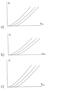
Answer: b
Explanation: A graph of IB against VBE is drawn. The curve so obtained is known as input characteristics. The collector emitter voltage (VCE) is kept constant.
32. The input resistance is given by _________
a) ∆VCE/∆IB
b) ∆VBE/∆IB
c) ∆VBE/∆IC
d) ∆VBE/∆IE
Answer: b
Explanation: The ratio of change in base emitter voltage (∆VBE) to resulting change in base current (∆IB) at constant collector emitter voltage (VCE) is defined as input resistance. This is denoted by ri.
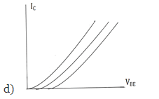
33. Which of the following depicts the output characteristics of a CE transistor?
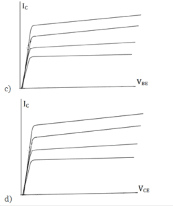
Answer: d
Explanation: A graph of IC against VCE is drawn. The curve so obtained is known as output characteristics. The base current (IB) is kept constant.
34. The output resistance is given by _________
a) ∆VCE/∆IB
b) ∆VBE/∆IB
c) ∆VBE/∆IC
d) ∆VCE/∆IC
Answer: d
Explanation: The ratio of change in collector emitter voltage (∆VCE) to resulting change in collector current (∆IC) at constant base current (IB) is defined as output resistance. This is denoted by ro.
35. Which of the following cases damage the transistor?
a) when VCE is increased too far
b) when VCE is decreased too far
c) when VBE is increased too far
d) when VBE is decreased too far
Answer: a
Explanation: When VCE is increased too far, collector base junction completely breaks down and due to this avalanche breakdown, collector current increases rapidly. This is not shown in the characteristic. In this case, the transistor is damaged.
36. When the collector junction is reverse biased and emitter junction is forward biased, the operating region of the transistor is called_________
a) inverted region
b) active region
c) cut off region
d) cut in region
Answer: b
Explanation: In the active region, for small values of base current, the effect of collector voltage over collector current is small while for large base currents this effect increases. The shape of characteristic here is same as that of CB transistors.
37. The small amount of current which flows even when base current IB=0 is called_________
a) IBEO
b) ICBO
c) ICEO
d) IC
Answer: c
Explanation: In the cut off region, a small amount of collector current flows even when base current IB is zero. This is called ICEO. Since the main current is also zero, the transistor is said to be cut off.
38. A change in 700mV in base emitter voltage causes a change of 200µA in the base current. Determine the dynamic input resistance.
a) 2kΩ
b) 10kΩ
c) 3kΩ
d) 3.5kΩ
Answer: c
Explanation: ro=∆VBE/∆IB
=700m/200µ=3.5kΩ.
39. The change in collector emitter voltage from 6V to 9V causes increase in collector current from 6mA to 6.3mA. Determine the dynamic output resistance.
a) 20kΩ
b) 10kΩ
c) 50kΩ
d) 60kΩ
Answer: b
Explanation: ro=∆VCE/∆IC
=3/0.3m=10kΩ.
40. Which of the following points locates the quiescent point?
a) (IC, VCB)
b) (IE, VCE)
c) (IE, VCB)
d) (IC, VCE)
Answer: a
Explanation: The quiescent point is best located between the cut off and saturation point. IE= VEE/RE, VCB=VCC-ICRL. It is denoted by ‘Q’.
41. The input resistance in a CB transistor is given by _________
a) ∆VCE/∆IB
b) ∆VBE/∆IB
c) ∆VBE/∆IC
d) ∆VEB/∆IE
Answer: d
Explanation: The ratio of change in emitter base voltage (∆VEB) to resulting change in emitter current (∆IE) at constant collector base voltage (VCB) is defined as input resistance. This is denoted by ri.
42. The output resistance of CB transistor is given by _________
a) ∆VCB/∆IC
b) ∆VBE/∆IB
c) ∆VBE/∆IC
d) ∆VEB/∆IE
Answer: a
Explanation: The ratio of change in collector base voltage (∆VCB) to resulting change in collector current (∆IC) at constant emitter current (IE)¬ is defined as output resistance. This is denoted by ro.
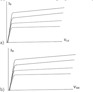
43. Which one of the following depicts the output characteristics for a CB transistor?
Answer: b
Explanation: A graph of IC against VCB is drawn. The curve so obtained is known as output characteristics. The emitter current (IE) is kept constant.
44. The input characteristics of a CE transistor is_________
a)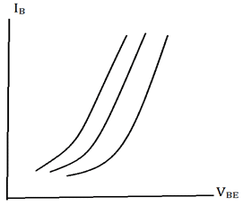
b)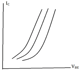
c) 
d) 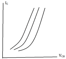
45. A transistor is connected in CB configuration. The emitter voltage is changed by 200mV, the emitter by 5mA. During this transition the collector base voltage is kept constant. What is the input dynamic resistance?
a) 30Ω
b) 60Ω
c) 40Ω
d) 50Ω
Answer: c
Explanation: The ratio of change in emitter base voltage (∆VEB) to resulting change in emitter current (∆IE) at constant collector base voltage (VCB) is defined as input resistance. This is denoted by ri.
We know, ∆VEB/∆IE=ri
=200/5=40Ω.
46. When the collector junction is reverse biased and emitter junction is forward biased, the operating region of the transistor is called_________
a) inverted region
b) active region
c) cut off region
d) cut in region
Answer: b
Explanation: In the active region, for small values of base current, the effect of collector voltage over collector current is small while for large base currents this effect increases. The shape of characteristic here is same as that of CB transistors.
47. Which of the following corresponds to the output circuit of a CB transistor?
a) VBE
b) IB
c) VCB
d) VCE
Answer: c
Explanation: Here, the quantity collector to base voltage corresponds to the output circuit of a CB transistor. The complete electrical behaviour of a transistor can be described by stating the relation between these quantities.
48. The input of a CB transistor is given between_________
a) collector and emitter terminals
b) base ad collector terminals
c) ground and emitter terminals
d) emitter and base terminals
Answer: d
Explanation: The name of the CB transistor says that it’s a common based one. The input is given between the emitter and base terminals and the output is taken between collector and base terminals.
49. The current gain of the CB transistor is_________
a) less than or equal to unity
b) equal to unity
c) greater than unity
d) remains same
Answer: a
Explanation: The input current flowing into the emitter terminal must be higher than the base current and collector current to operate the transistor. Therefore the output collector current is less than the input emitter current.
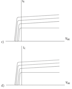
50. The input characteristics of a CB transistor resembles_________
a) Forward biased diode
b) Illuminated photo diode
c) LED
d) Zener diode
Answer: b
Explanation: The input characteristics resemble the illuminated photo diode and the output characteristics resemble the forward biased diode. This transistor has low input impedance and high output impedance.
51. Which of the following depicts the DC load line?
a) 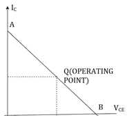
b) 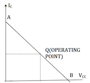
c) 
d) 
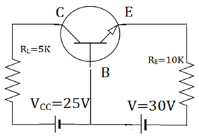
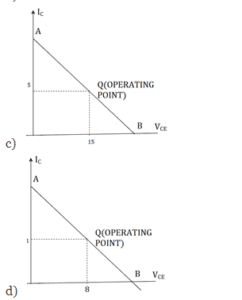
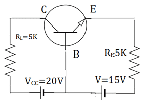
52. For the circuit shown, find the quiescent point.
a) (10V, 4mA)
b) (4V, 10mA)
c) (10V, 3mA)
d) (3mA, 10V)Answer: c
Explanation: We know, IE=VEE/RE=30/10kΩ=3mA
IC=α IE =IE =3mA
VCB=VCC-ICRL=25-15=10V. So, quiescent point is (10V, 3mA).
53. Which of the following depicts the load line for the circuit shown below?
a) 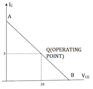
b) 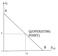
c)
d)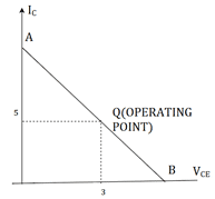
Answer: d
Explanation: We know, IE=VEE/RE=15/5kΩ=3mA
IC=α IE =IE =3mA
VCB=VCC-ICRL=20-15=5V. So, quiescent point is (5V, 3mA).
54. For the circuit shown, find the quiescent point.
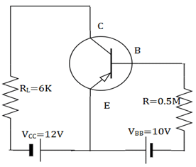
a) (6V, 1mA)
b) (4V, 10mA)
c) (10V, 3mA)
d) (3mA, 10V)
Answer: c
Explanation: We know, VCE=12V
(IC)SAT =VCC/RL=12/6K=2mA. IB=10V/0.5M=20µA. IC= βIB=1mA. I
VCE=VCC-ICRL=12-1*6=6V. So, quiescent point is (6V, 1mA).
55. Which of the following depicts the load line for the given circuit?
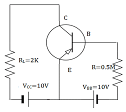
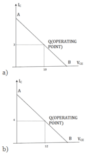
Answer: d
Explanation: We know, VCE=6V
(IC)SAT =VCC/RL=10/2K=5mA. IB=10V/0.5M=20µA. IC= βIB=1mA. I
VCE=VCC-ICRL=10-1*2=8V. So, quiescent point is (8V, 1mA).
56. The DC equivalent circuit for an NPN common base circuit is.
57. The DC equivalent circuit for an NPN common emitter circuit is.


59. What is the DC characteristic used to prove that the transistor is indeed biased in saturation mode?
a) IC = βIB
b) IC > βIB
c) IC >> βIB
d) IC < βIBAnswer: d
Explanation: When in a transistor is driven into saturation, we use VCE(SAT) as another linear parameter. In, addition when a transistor is biased in saturation mode, we have IC < βIB. This characteristic used to prove that the transistor is indeed biased in saturation mode.
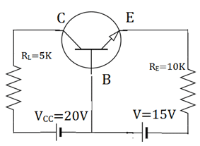
60. For the circuit shown, find the quiescent point.
a) (10V, 4mA)
b) (4V, 10mA)
c) (10V, 3mA)
d) (3mA, 10V)Answer: c
Explanation: We know, IE=VEE/RE=10/5kΩ=2mA
IC=α IE =IE =2mA
VCB=VCC-ICRL=20-10=10V. So, quiescent point is (10V, 2mA).
61. In which of the following configuration does a MOSFET works as an amplifier?
a) Common Source (CS)
b) Common Gate (CG)
c) Common drain (CD)
d) All of the mentioned
Answer: d
Explanation: There are three basic configurations for connecting the MOSFET as an amplifier. Each of these configurations is obtained by connecting one of the three MOSFET terminals to ground, thus creating a two-port network with the grounded terminal being common to the input and output ports.
62. The MOSFET in the following circuit is in which configuration?
a) Common Source (CS)
b) Common Gate (CG)
c) Common Drain (CD)
d) None of the mentioned
Answer: b
Explanation: It is the circuit for Common gate configuration.
63. The MOSFET in the following circuit is in which configuration?
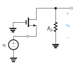
a) Common Source (CS)
b) Common Gate (CG)
c) Common Drain (CD)
d) None of the mentioned
Answer: c
Explanation: It is the circuit for Common drain configuration.
64. The MOSFET in the following circuit is in which configuration?[/expand] 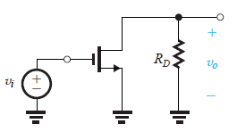
a) Common Source (CS)
b) Common Gate (CG)
c) Common Drain (CD)
d) None of the mentionedAnswer: a
Explanation: It is the circuit for Common source configuration.
(Q.65-Q.70) Reference circuit for Q.5-Q.10 The circuit below is the characterization for the amplifier as a functional block.
65. If the value of Rin for the common source configuration is R1 and that for common source with a source resistance configuration is R2 ideally. The ratio of R1/R2 will be
a) R1/R2 = 1
b) 0 < R1/R2 < 1
c) R1/R2 > 1
d) R1/R2 = 0
Answer: a
Explanation: Ideally both must have infinite resistance.
66. Which is true for the value of Avo for common source (Represented by A1) and common source with a source resistance (represented by A2).
a) A1 = A2
b) A1 > 2
c) A1 < A2
d) |A1| < |A2|
Answer: c
Explanation: A1 = -gmRD and A2 = -gmRD/1+gmRS
Reference circuit for Common source configuration
Reference circuit for common source with source resistance RS
70. Which of the following has AVO independent of the circuit elements?
a) Common source configuration
b) Common gate configuration
c) Source follower configuration
d) None of the mentioned
Answer: c
Explanation: AVO = 1 source follower.
71. If a MOSFET is to be used in the making of an amplifier then it must work in
a) Cut-off region
b) Triode region
c) Saturation region
d) Both cut-off and triode region can be used
Answer: c
Explanation: Only in the saturation region a MOSFET can operate as an amplifier.
72. For MOSFET is to be used as a switch then it must operate in
a) Cut-off region
b) Triode region
c) Saturation region
d) Both cut-off and triode region can be used
Answer: d
Explanation: In both regions it can perform the task of a switch.
(Q73 & Q.74) Using the circuit shown below,
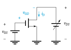
73. Determine the conditions in which the MOSFET is operating in the triode region.
i. VGD > Vt (Threshold voltage)
ii. VDS > VOV
iii. ID ∝ (VOV – 0.5VDS)VDS
a) i, ii, and iii are correct
b) i and iii are correct
c) i and ii are correct
d) ii and iii are correct
Answer: b
Explanation: Only the points I and iii are correct and ii is false.
74. Determine the conditions in which the MOSFET is operating in the saturation region
i. VGD > Vt (Threshold voltage)
ii. VDS > VOV
iii. ID ∝ (VOV)2
a) i, ii, and iii are correct
b) i and iii are correct
c) i and ii are correct
d) ii and iii are correct
Answer: d
Explanation: i is false and ii and iii are true.
75. In the saturation region of the MOSFET the saturation current is
a) Independent of the voltage difference between the source and the drain
b) Depends directly on the voltage difference between the source and the drain
c) Depends directly on the overdriving voltage
d) Depends directly on the voltage supplied to the gate terminal
Answer: a
Explanation: Saturation current does not depends on the voltage difference between the source and the drain in the saturation region of a MOSFET.
76. An n-channel MOSFET operating with VOV=0.5V exhibits a linear resistance = 1 kΩ when VDS is very small. What is the value of the device transconductance parameter kn?
a) 2 mA/V2
b) 20 mA/V2
c) 0.2 A/V2
d) 2 A/V2
Answer: a
Explanation: Use the standard mathematical expression to determine the value of kn.
77. An NMOS transistor is operating at the edge of saturation with an overdrive voltage VOV and a drain current ID. If is VOV is doubled, and we must maintain operation at the edge of saturation, what value of drain current results?
a) 0.25ID
b) 0.5ID
c) 2ID
d) 4ID
Answer: c
Explanation: I0 is directly proportional to VOS.
(Q.78-Q.80) Using the circuit below answer the question
78. Which of the following is true for the triode region?
a. VDG > Vtp
b. VSD < VOV
c. ID ∝ VOV
d. None of the mentioned
Answer: d
Explanation: VDG > |Vtp| and VSD < |VOV|.
79. Which of the following is true for the saturation region?
a) VDG ≤ |Vtp|
b) VSD ≤| VOV|
c) VDG < |Vtp|
d) VSD <| VOV|Answer: a
Explanation: It is a characteristic for the saturation region.
80. The current iD
a) Depends linearly on VOV in the saturation region
b) Depends on the square of VOV in the saturation region
c) Depends inversely on VOV in the triode region
d) None of the mentioned
Answer: b
Explanation: Use the standard mathematical expressions for i0 in different regions.
1. The feature of an approximate model of a transistor is
a) it helps in quicker analysis
b) it provides individual analysis for different configurations
c) it helps in dc analysis
d) ac analysis is not possible
Answer: a
Explanation: The small signal model helps in quicker ac analysis of a transistor. The approximate model is applicable for all the configurations. The dc analysis is not obtained by using a small signal model of transistor.
2 A transistor has hfe=100, hie=2kΩ, hoe=0.005mmhos, hre=0. Find the output impedance if the lad resistance is 5kΩ.
a) 5kΩ
b) 4kΩ
c) 20kΩ
d) 15kΩ
Answer: b
Explanation: RO=I/hoe=1/0.005m
=20kΩ.ROI= RO || RLI=20||5
=4kΩ.
3. A CE amplifier when bypassed with a capacitor at the emitter resistance has
a) increased input resistance and increased voltage gain
b) increased input resistance and decreased voltage gain
c) decreased input resistance and increased voltage gain
d) decreased input resistance and decreased voltage gain
4. A transistor has hie =2kΩ, hoe=25µmhos and hfe=60 with an unbypassed emitter resistor Re=1kΩ. What will be the input resistance and output resistance?
a) 90kΩ and 50kΩ respectively
b) 33kΩ and 45kΩ respectively
c) 6kΩ and 40kΩ respectively
d) 63kΩ and 40kΩ respectively
Answer: d
Explanation: As the emitter is unbypassed, the input resistance Ri=hie+(1+hfe)Re
=2+61=63kΩ. The output resistance RO=1/hoe=1/25MΩ=40kΩ.
5. A transistor has hie =1KΩ and hfe=60 with an bypassed emitter resistor Re=1kΩ. What will be the input resistance and output resistance?
a) 90kΩ and 50kΩ respectively
b) 33kΩ and 45kΩ respectively
c) 6kΩ and 40kΩ respectively
d) 63kΩ and 40kΩ respectively
Answer: d
Explanation: As the emitter is bypassed, the input resistance Ri=hie
=1kΩ. The output resistance RO=1/hoe but the value is not given.
So, hoe=0 and RO=1/0=∞.
6. In the given circuit, find the equivalent resistance between A and B nodes.
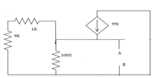
a) 100kΩ
b) 50kΩ
c) 40kΩ
d) 60kΩ
Answer: b
Explanation: RAB=RO||100Ω
= (RSI+hie/1+hfe)||100
=9+1/100||100=100||100=50Ω.
7. Which of the following acts as a buffer?
a) CC amplifier
b) CE amplifier
c) CB amplifier
d) cascaded amplifier
Answer: a
Explanation: The voltage gain of a common collector amplifier is unity. It is then used as a buffer. The CC amplifier is also called as an emitter follower. Though there is no amplification done, the output will be stabilised.
8. Which of the following is true?
a) CC amplifier has a large current gain
b) CE amplifier has a large current gain
c) CB amplifier has low voltage gain
d) CC amplifier has low current gain
Answer: b
Explanation: The CE amplifier has high current and voltage gains. The CC amplifier has unity voltage gain which cannot be regarded as high. The common base amplifier has a unity current gain and high voltage gain.
9. In an NPN silicon transistor, α=0.995, IE=10mA and leakage current ICBO=0.5µA. Determine ICEO.
a) 10µA
b) 100µA
c) 90µA
d) 500µA
Answer: b
Explanation: IC=α IE +ICBO =0.995*10mA+0.5µA=9.9505mA.
IB=IE-IC=10-9.9505=0.0495mA. β=α/(1-α)=0.995/(1-0.995)=199
ICEO=9.9505-199*0.0495=0.1mA==100µA.
10. In CB configuration, the value of α=0.98A. A voltage drop of 4.9V is obtained across the resistor of 5KΩ when connected in collector circuit. Find the base current.
a) 0.01mA
b) 0.07mA
c) 0.02mA
d) 0.05mA
Answer: c
Explanation: Here, IC=4.9/5K=0.98mA
α = IC/IE .So,
IE=IC/α=0.98/0.98=1mA.
IB=IE-IC=1-0.98=0.02mA.
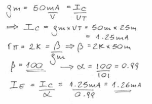
11. A transistor with ß = 120 is biased to operate at a dc collector current of 1.2 mA. Find the value of gm.
a) 12mA/V
b) 24 mA/V
c) 36 mA/V
d) 48 mA/V
Answer: d
Explanation:

12. A transistor with ß = 120 is biased to operate at a dc collector current of 1.2 mA. Find the value of R?p.
a) 625 ohm
b) 1250 ohm
c) 2500 ohm
d) 5000 ohm
Answer: c
Explanation:
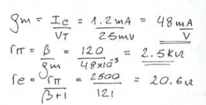
13. A transistor with ß = 120 is biased to operate at a dc collector current of 1.2 mA. Find the value of Re.
a) 2.5 ohm
b) 20.6 ohm
c) 25.2 ohm
d) 30.4 ohm
Answer: b
Explanation:

14. A transistor operating with nominal gm of 60 mA/V has a ß that ranges from 50 to 200. Also, the bias circuit, being less than ideal, allows a 20% variation in Ic. What is the smallest value found of the resistance looking into the base?
a) 347 ohm
b) 694 ohm
c) 1041 ohm
d) 1388 ohm
Answer: b
Explanation:
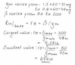
15. A transistor operating with nominal gm of 60 mA/V has a ß that ranges from 50 to 200. Also, the bias circuit, being less than ideal, allows a 20% variation in Ic. What is the largest value found of the resistance looking into the base?
a) 1050 ohm
b) 21000 ohm
c) 3150 ohm
d) 4200 ohm
Answer: d
Explanation:

16. A designer wishes to create a BJT amplifier with a gm of 50 mA/V and a base input resistance of 2000 O or more. What is the minimum ß he can tolerate for the transistor used?
a) 100
b) 150
c) 200
d) 250
Answer: a
Explanation:

17. A designer wishes to create a BJT amplifier with a gm of 50 mA/V and a base input resistance of 2000 O or more. What emitter bis current should he choose?
a) 1.06 mA
b) 1.16 mA
c) 1.26 mA
d) 1.36 mA
Answer: c
Explanation:
18. Which of the following is true?
a) Ib = ß Ic
b) Ib = ß + 1/ Ic
c) Ib = Ic/ß
d) Ib = Ic/ ß – 1
Answer: c
Explanation: The correct relationship between Ic and Ie is Ib = Ic/ß.
19. The SI units of transconductance is
a) Ampere/ volt
b) Volt/ ampere
c) Ohm
d) Siemens
Answer: a
Explanation: Transcoductance is given by Ic/Vt.
20. Which of the following represents the correct mathematical form of the term denoted by the symbol Rp?
a) ß/gm
b) Vt/Ib
c) All of the mentioned
d) None of the mentioned
Answer: c
Explanation: Both of the expressions are identical.
21. The current gain of BJT is_________
a) gmro
b) gm/ro
c) gmri
d) gm/ri
Answer: c
Explanation: We know, current gain AV=hfe. In π model, hfe is referred to β.
We know, ri= β/gm.
From this, β=rigm.
22. For the amplifier circuit of fig. The transistor has β of 800. The mid band voltage gain VO/VI of the circuit will be_________
a) 0
b) <1
c) =1
d) 800
Answer: c
Explanation: The circuit is PNP transistor, collector coupled amplifier. The voltage gain is unity for a CC amplifier. Hence on observation, the CC amplifier gives a unity gain.
23. In a bipolar transistor at room temperature, the emitter current is doubled the voltage across its base emitter junction_________
a) doubles
b) halves
c) increase by about 20mV
d) decreases by about 20mV
Answer: c
Explanation: The change in voltage with temperature can be found by, V(T) = 2.3m(∆T)VO . In a bipolar transistor at room temperature if the emitter current is doubled the voltage across its base emitter junction thereby doubles.
24. A common emitter transistor amplifier has a collector current of 10mA, when its base current is 25µA at the room, temperature. What is input resistance?
a) 3kΩ
b) 5kΩ
c) 1kΩ
d) 7kΩ
Answer: c
Explanation: We know, β/gm=ri
= (IC/IB)/(IC/VT)=VT/IB=25m/25µ=1k.
25. For an NPN transistor connected as shown in below, VBE=0.7V. Give that reverse saturation current of junction at room temperature is 10-13A, the emitter current is_________
a) 30mA
b) 39mA
c) 29mA
d) 49mA
Answer: d
Explanation: When the collector and base are shorted, the transistor behaves as a normal diode. So, the diode equations imply. IE=IO(eV/V0-1). We get, IE=49mA.
26. The voltage gain of given circuit below is_________
a) 100
b) 20
c) 10
d) 30
Answer: c
Explanation: The gain for the given circuit can be found by, AV=RF/RS
=100K/10K=10.
27. A small signal source V(t)=Acos20t+Bsin10000t, is applied to a transistor amplifier as shown. The transistor has β=150 and hie=3KΩ. What will be the VO?
a) 1500(Acos20t+Bsin10000t)
b) -150(Acos20t+Bsin10000t)
c) -1500Bsin10000t
d) -150Bsin10000t
Answer: d
Explanation: AV=-hfe RLI/hie=3*150/3=-150. So, VO=-150V(t)
But cos20t has low frequency so capacitors are open circuited. Only, the sine component is allowed.
So, Vo =-150Bsin10000t.
28. Which of the following statements are correct for basic transistor configurations?
a) CB Amplifiers has low input impedance and low current gain
b) CC Amplifiers has low input impedance and high current gain
c) CE Amplifiers has very poor voltage gain but very high input impedance
d) The current gain of CB Amplifier is higher than the current gain of CC Amplifiers
Answer: a
Explanation: The CE amplifier has moderate input and output impedances. The CC amplifier has unity voltage gain. The common ba se amplifier has a unity current gain and high voltage gain.
29. The collector current is 2.945A and α=0.98. The leakage current is 2µA. What is the emitter current and base current?
a) 3mA and 55µA
b) 2.945mA and 55µA
c) 3.64mA and 33µA
d) 5.89mA and 65µA
Answer: a
Explanation: (IC – ICBO)/α=IE
= (2.945-0.002)/0.98=3mA.
IE=IC+IB . So, IB=3-2.495=0.055mA=55µA.
30. The change in collector emitter voltage from 6V to 9V causes increase in collector current from 6mA to 6.3mA. Determine the dynamic output resistance.
a) 20kΩ
b) 10kΩ
c) 50kΩ
d) 60kΩ
Answer: b
Explanation: ro=∆VCE/∆IC
=3/0.3m=10kΩ.
31. A transistor is connected in CB configuration. The emitter voltage is changed by 200mV, the emitter by 5mA. During this transition the collector base voltage is kept constant. What is the input dynamic resistance?
a) 30Ω
b) 60Ω
c) 40Ω
d) 50Ω
View Answer
32. Which type of amplifiers exhibits the current gain approximately equal to unity without any current amplification?
a) CE
b) CB
c) CC
d) Cascade
Answer: b
Explanation: In common base amplifier, input signal is applied at emitter terminal while the amplified output signal is obtained at the collector terminal with respect to ground.
For the AC signals, the base terminal is specifically connected to ground through the capacitor.
Even, the output resistance is very high & hence, the current gain is approximately equal to unity. Due to this, there is no possibility of current amplification. Consequently, the CB amplifier exhibits high voltage gain.
33. Why is the Darlington configuration not suitable for more than two transistors?
a) Because leakage current increases and voltage gain decreases with multiple numbers of transistors
b) Because leakage current decreases and voltage gain increases with multiple numbers of transistors
c) Because leakage current as well as voltage gain increases with multiple numbers of transistors
d) Because leakage current as well as voltage gain decreases with multiple numbers of transistors
Answer: a
Explanation: As the number of transistors increases, the leakage current also increases. The leakage current gets multiplied by the current gain of Darlington configuration.
Generally, the voltage gain of CC configuration is nearly equal to ‘1’ but the voltage gain of Darlington configuration is very less than ‘1’.
Therefore, if we increase the number of transistors in Darlington configuration the voltage gain will ultimately reduce. But, in order to prevent these likely undesirable conditions, Darlington configuration is completely inappropriate for more than two transistors.
34. What should be the level of input resistance to allow the occurrence of source loading in common base amplifier configuration?
a) low
b) high
c) moderate
d) stale
Answer: a
Explanation: As per the configuration of CB amplifier, it is evident that its input resistance is very low but its output resistance is enormously high.
However, the lower value of input resistance allows the stipulation of source loading in common base amplifier circuit.
Thus, there is no current amplification because of unity current gain. These all reasons eventually add to high level of voltage gain.
35. Which among the below assertions is not a relevant property of CE amplifier?
a) High voltage gain
b) High current gain
c) High input resistance
d) High output resistance
Answer: d
Explanation: The voltage gain, current gain and input resistance CE amplifiers are utterly high but it has low output resistance.
The collector resistor (Rc) performs the purpose of controlling the collector current. Input and emitter resistors are adopted for biasing of transistor in an active region so that it becomes possible for the transistor to function as an amplifier.
Due to high current gain at the output of RC coupled CE amplifier, the resistance level at the output is exceedingly low.
36. What is the phase-shift between input and output voltages of CE amplifier?
a) 90°
b) 120°
c) 180°
d) 270°
Answer: c
Explanation: During the amplification method of RC coupled CE amplifier, there is a phase shift of about 180o between input and output. Basically, the output is said to be reversed version of input.
The magnitude of output voltage becomes higher as compared to that of input signal but the shape is correctly similar to that of an input signal.
But, the input ac signal gets amplified along with the phase-shift of 180o between input and output.
37. Which capacitor is used to block DC portion by allowing to pass only AC portion of the amplified signal to load?
a) Input Coupling Capacitor
b) Bypass Capacitor
c) Output Coupling Capacitor
d) Both coupling and bypass capacitor
Answer: c
Explanation: In RC coupled CE amplifier, the transistor is connected in common-emitter (CE) configuration and capacitors C1 & C2 are coupling capacitors.
Input coupling capacitor is used for coupling the ac input voltage to the transistor base. Inversely, the output coupling capacitor (C2) is used for coupling an output of an amplifier to the load resistance or to the next stage of an amplifier.
Besides these, input coupling capacitor blocks any DC element present in AC input voltage & couples only AC component of input signal whereas bypass capacitor offers a low reactance to the amplified AC signal.
38. The configuration in which voltage gain of transistor amplifier is lowest is ____________
a) common collector
b) common emitter
c) common base
d) common emitter & base
Answer: a
Explanation: In common collector configuration (also known as the emitter follower) because the emitter voltage follows that of the base. Offering a high input impedance and a low output impedance it is extensively used as a buffer. The voltage gain is unity, even though current gain is high. The input and output signals are in phase.
39. The configuration in which current gain of transistor amplifier is lowest is ___________
a) common collector
b) common base
c) common emitter
d) common emitter & base
Answer: b
Explanation: In Common base configuration, the input impedance is very low; While offering a high output impedance. Although the voltage is high, the current gain is low and the overall power gain is also low when compared to the other transistor configurations available. Thus, there is no current amplification because of unity current gain.
40. The configuration in which input impedance of transistor amplifier is lowest is ___________
a) common collector
b) common emitter
c) common base
d) common emitter & base
Answer: c
Explanation: In Common base configuration, the input impedance is very low; While offering a high output impedance. Although the voltage is high, the current gain is low and the overall power gain is also low when compared to the other transistor configurations available.
41. The configuration in which output impedance of transistor amplifier is highest is ___________
a) common collector
b) common base
c) common emitter
d) common collector and base
Answer: b
Explanation: In Common base configuration, the input impedance is very low; While offering a high output impedance. Although the voltage is high, the current gain is low and the overall power gain is also low when compared to the other transistor configurations available.
42. Q. What should be the gain of an amplifier at 20 kHz if the half power frequencies are fL = 20 Hz and fH = 15 kHz along with mid band gain = 80?
a) 22.76
b) 45.09
c) 40.08
d) 48.07
Answer: d
Explanation:
fL = 20 Hz
fH = 15 kHz
Av(mid) = 80
To determine: Voltage gain at 20 kHz
Formula : Av = Av(mid) / √1 + (f/fH)2
To determine the voltage gain at 20 kHz, we recognize that,
Av = Av(mid) / √1 + (f/fH)2
= 80 / √1 + (20 k/15k)2
= 48.07.
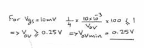
42. An NMOS technology has μnCox = 50 μA/V2 and Vt = 0.7 V. For a transistor with L = 1μm, find the value of W that results in gm 1mA/V at ID = 0.5 mA.
a) 10 μm
b) 20 μm
c) 30 μm
d) 40 μm
Answer: b
Explanation:
43. Consider an NMOS transistor having kn= 2 mA/V2. Let the transistor be biased at VOV = 1V. For operation in saturation, what dc bias current ID results? If a +0.1-V signal is superimposed on VGS, find the corresponding increment in collector current by evaluating the total collector current ID and subtracting the dc bias current ID.
a) ID = 1mA and Increment = 0.21 mA
b) ID = 1mA and Increment = 0.42 mA
c) ID = 2mA and Increment = 0.21 mA
d) ID = 2mA and Increment = 0.42 mA
Answer: a
Explanation:
44. We know ID =1/2 kn (VGS + vgs – Vt)2. Let the signal vgs be a sine wave with amplitude Vgs, and substitute vgs = Vgs sin ω t in Eq.(5.43). Using the trigonometric identity show that the ratio of the signal at frequency 2ω to that at frequency ω , expressed as a percentage (known as the second-harmonic distortion) is
a) Vgs/Vov x 100%
b) 1/2Vgs/Vov x 100%
c) 1/4Vgs/Vov x 100%
d) 1/8Vgs/Vov x 100%
Answer: c
Explanation:
45. If in a particular application Vgs is 10 mV, find the minimum overdrive voltage at which the transistor should be operated so that the second-harmonic distortion is kept to less than 1%.
a) 1V
b) 0.75V
c) 0.5V
d) 0.25V
Answer: d
Explanation:
(Q.46-Q.48) An NMOS amplifier is to be designed to provide a 0.50-V peak output signal across a 50-kΩ load that can be used as a drain resistor.
46. If a gain of at least 5 V/V is needed, what value of gm is required?
a) 0.1 mA/V
b) 0.2 mA/V
c) 0.4 mA/V
d) 0.8 mA/V
Answer: a
Explanation: gmRd = 5 or gm= 5/50 mA/V.
47. Using a dc supply of 3 V, what values of ID and VOV would you choose?
a) 0.34 mA and 0.35 V respectively
b) 0.34 mA and 0.69 V respectively
c) 0.034 mA and 0.35 V respectively
d) 0.034 mA and 0.69 V respectively
Answer: d
Explanation:
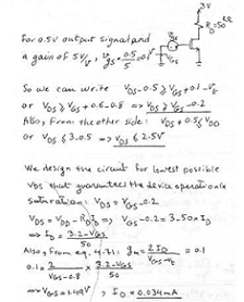
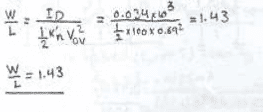
48. What W/L ratio is required if μnCox = 200 μA/V2?
a) 1.23
b) 1.23
c) 1.43
d) 1.53
Answer: c
Explanation:
(Q.49-Q.50) For a 0.8-μm CMOS fabrication process: Vtn= 0.8 V, Vtp = −0.9 V, μnCox = 90 μA/V2, μpCox = 30 μA/V2, Cox = 1.9 fF/μm2, VA (n-channel devices) = 8L (μm), and |VA| (p-channel devices) = 12L (μm).
49. Find the small-signal model parameters (gm, ro and gmb) for an NMOS transistor having W/L = 20 μm/2 μm and operating at ID = 100 μA and |VSB| = 1V.
a) gm= 0.42mA/V, ro= 160 kΩ, gmb = 0.084 mA/V
b) gm= 0.21mA/V, ro= 160 kΩ, gmb= 0.042 mA/V
c) gm= 0.42mA/V, ro= 80 kΩ, gmb = 0.042 mA/V
d) gm= 0.24mA/V, ro= 80 kΩ, gmb = 0.084 mA/V
Answer: a
Explanation:
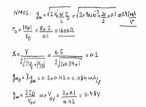
50. Find the small-signal model parameters (gm, ro and gmb) for a PMOS transistor having W/L = 20 μm/2 μm and operating at ID = 100 μA and |VSB| = 1V.
a) gm= 0.24mA/V, ro= 240 kΩ, gmb = 0.024 mA/V
b) gm= 0.24mA/V, ro= 120 kΩ, gmb = 0.048 mA/V
c) gm= 0.24mA/V, ro=240 kΩ, gmb = 0.048 mA/V
d) gm= 0.12mA/V, ro= 240 kΩ, gmb = 0.048 mA/V
Answer: c
Explanation:
51. The overdrive voltage at which each device must be operating is
a) NMOS = 0.83V and PMOS = 0.48V
b) NMOS = 0.48V and PMOS = 0.83V
c) NMOS = 0.24V and PMOS = 0.41V
d) NMOS = 0.41V and PMOS = 0.24V
Answer: b
Explanation:
NMOS case
![]()
PMOS case
52. The frequency response of transformer coupling is ________
a) Good
b) Very Good
c) Excellent
d) Poor
Answer: d
Explanation: The transformer coupling has a poor frequency response. The gain varies considerably with frequency. The gain is constant only over small range of frequencies. Thus transformer coupling introduces frequency distortion; due to which its frequency response is poor.
53. What is the purpose of RC or transformer coupling?
a) To block a.c.
b) To separate bias of one stage from another
c) Increase thermal stability
d) Increase Efficiency
Answer: b
Explanation: In RC or transformer coupling, a capacitor / transformer is used as coupling device which connects output of first stage with input of second stage. Its function is to pass the a.c signal and blocks d.c. bias voltage.
54. Why is RC coupling confined to low power applications?
a) Due to large value of coupling capacitor
b) Low efficiency
c) Large number of components
d) Due to is frequency response
Answer: b
Explanation: RC coupled amplifiers have low voltage and power gain. It is because the low resistance presented by the input of each stage to the preceding stage decreases the effective load resistance and hence the gain. Thus its efficiency is reduced.
55. A radio receiver has how many stages of amplification?
a) One
b) Two
c) Three
d) More than one
Answer: d
Explanation: A multistage amplifier circuit affects the high input impedance of a common source stage combined with the input to output isolation of a common gate stage. A radio receiver has more than one stage of amplification because it is required to restore the characteristics of a radio signal over various channels.
56. Which of the following is an advantage of RC coupling scheme?
a) Good impedance matching
b) Economy
c) High efficiency
d) Frequency response
Answer: b
Explanation: It uses the resistor and capacitor which are not expensive so the cost is low. But it has poor impedance matching because its output impedance is several times larger than the device; at its terminal end. It is unsuitable for low frequency application.
57. The voltage gain is practically expressed in _______
a) db
b) volts
c) as a number
d) ampere
Answer: a
Explanation: Db scale is logarithmic. Voltage gain increases exponentially with frequency so using a linear scale means that we need to work with large values of gain, corresponding to small values of frequency.
58. If a three stage amplifier has individual stage gains of 10db, 6db and 15db; then the total gain in db is ______
a) 600db
b) 24db
c) 14db
d) 31db
Answer: d
Explanation: The overall gain of a multistage amplifier is given as the product of the gain of the individual stages.
Gain (A) = A1 * A2 * A3 ……* An
Alternately, if the gain of each stage is given in db
The overall gain of the amplifier is the sum of gain of each stage
Gain in db = A1 + A2 + A3 (db)
= 10+6+15 = 31db.
59. For extremely low frequencies, RC coupling is not used because of ___________
a) There is considerable power loss
b) There is a hum in the output
c) Electrical size of the coupling capacitor
d) Low efficiency
Answer: c
Explanation: Xc = the electrical size of coupling capacitor
Relation of Xc with the signal frequency (f):
Xc = 1 \Xc is inversely proportional to f.
At low frequencies, Xc becomes very large; output reactance of capacitor increases.
The voltage across load resistance also reduces because some voltage drop takes place across Xc.
Thus output voltage reduces. Therefore gain is very low.
60. Which transformer is used for impedance matching in transistor coupled amplifier?
a) step-up
b) step-down
c) same turn ratio
d) different turn ratio
Answer: b
Explanation: Usually the impedance of an output device is a few ohms whereas output impedance of the transistor is several 100 ohms. In order to match the impedance a step down transformer of proper turn’s ratio is used. The impedance of secondary of the transformer is made equal to the load impedance and primary impedance equal to the output impedance of the transistor.
61. Gain of an amplifier usually expressed in db because _______________
a) It is a small unit
b) Calculations become easy
c) Human ear response is logarithmic
d) Gain is reduced
Answer: c
Explanation: The human hearing scale is logarithmic in nature. For doubling perceived intensity of sound, the sound power must be increased by 10 times. That means the gain of amplifier which controls sound intensity must have gain of 10 for doubling perceived intensity of sound which is in a bell and in 10 decibel scale.
62. The total gain of a multistage amplifier is less than the product of the gains of individual stages due to ___________
a) Power loss in the coupling device
b) Loading effect of the next stage
c) The use of many transistors
d) The use of many capacitors
Answer: b
Explanation: The output of first amplifier stage is the input to next stage. In this way overall voltage gain can be increased, when number of amplifier stage is used in succession, it is called a multistage amplifier. The load of first amplifier is the input resistance of the second amplifier. Thus overall gain is reduced.+
1. In Miller’s theorem, what is the constant K?
a) Total voltage gain
b) Internal voltage gain
c) Internal current gain
d) Internal power gain
Answer: b
Explanation: The constant K=V2/V1, which is the internal voltage gain of the network.
Thus resistance RM=R/1-K
RN=R/1-K-1.
2. When applying miller’s theorem to resistors, resistance R1 is for node 1 and R2 for node 2. If R1>R2, then for same circuit, then for capacitance for which the theorem is applied, which will be larger, C1 or C2?
a) C1
b) C2
c) Both are equal
d) Insufficient data
Answer: a
Explanation: Given R1>R2
R/1-K > R/1-K-1, and so 1-K-1>1-K
Thus K2>1, K>1, K<-1 (correct)
Thus, C1=C(1-K) and C2=C(1-K-1)
Hence C1>C2
3. Find net voltage gain, given hfe = 50 and hie = 1kΩ.
a) 27.68
b) -22
c) 30.55
d) -27.68
Answer: d
Explanation: Apply millers theorem to resistance between input and output.
At input, RM=100k/1-K = RI
Output, RN=100k/1-K-1 ≈ 100k
Internal voltage gain , K = -hfeRL’/hie
K = – 50xRc||100k/1k = – 50x4x100/104= – 192
RI = 100k/1+192 = 0.51kΩ
RI’ = RI||hie = 0.51k||1k = 0.51×1/1.51 = 0.337kΩ
Net voltage gain = K.RI’/RS+RI’ = – 192 x 0.337/2k + 0.337k = -27.68.
4. Given that capacitance w.r.t the input node is 2pF and output node is 4pF, find capacitance between input and output node.
a) 0.67 pF
b) 1.34pF
c) 0.44pF
d) 2.2pF
Answer: a
Explanation: C1=C(1-K), C2=C(1-K-1)
C1=2pF
C2=4pF
C1/C2=1/2=1-K/1-K-1
K = -2
C1 = C(1+2) = 3C
C = C1/3 = 2/3pF = 0.67 pF.
5. Consider an RC coupled amplifier at low frequency. Internal voltage gain is -120. Find the voltage gain magnitude, when given that collector resistance = 1kΩ, load = 9kΩ, collector capacitance is 0. is 0.1μF, and input frequency is 20Hz.
a) 120
b) 12
c) 15
d) -12
Answer: c
Explanation: AV = -120
fL = 1/2πCC(RC+RL) = 1/2π*0.001 = 1000/2π = 159.15Hz
AV’ = |AV|1√+(fLf)2
AV’ = 120/8.02 ≈ 15.
6. Find the 3-dB frequency given that the gain of RC coupled amplifier is 150, the low frequency voltage gain is 100 and the input frequency is 50Hz.
a) 50.8 Hz
b) 55.9 Hz
c) 60Hz
d) 100Hz
Answer: b
Explanation: AVM = 150
AVL = 100
f = 50Hz
100 = 1501√+(fL50)2
1+f2/2500 =1.52
f2 = 2500*1.25 = 3125
f = 55.90 Hz.
7. Given collector resistance = 2kΩ, load resistance = 5kΩ, collector capacitance = 1μF, emitter capacitance = 20μF, collector current = 2mA, source resistance = 2kΩ. If the effect of blocking capacitor is ignored, find the applicable cut-off frequency.
a) 22.73 Hz
b) 612 Hz
c) 673Hz
d) 317 Hz
Answer: b
Explanation: RC = 2kΩ, RL = 5kΩ, CC = 1μF, CB = 10μF, CE = 20μF, RS = 2 kΩ
hie = 1kΩ, IC = 2mA
fL1 = 1/2πCC(RC+RL) = 22.73 Hz
fL2 = gm/2πCE = IC/2πCEVT = 612 Hz
Since fL2 > 4fL1, hence fL2 is the correct answer.
8. Consider the circuit shown.
hfe = 50, hie = 1000Ω. Find magnitude of voltage gain at input frequency 10Hz.
a) 100
b) 133
c) 166
d) 220
Answer: b
Explanation: Net load = 10k||10k = 5kΩ = RL’
AVM = -hfeRL’/hie = -50×5/1 = -250
fL = 1/2πCC(RC+RL) = 15.9 Hz
AVL = AVM1√+(fLf)2 = 133.
9. What is the phase shift in RC coupled CE amplifier at lower 3dB frequency?
a) 180°
b) 225°
c) 270°
d) 100°
Answer: b
Explanation: Total phase shift = 180°+ tan-1(fL/f)
At 3dB frequency fL/f = 1
Total phase shift = 180° + 45° = 225°.
10. Consider that the phase shift of an RC coupled CE amplifier is 260°. Find the low frequency gain when the voltage gain of the transistor is -150.
a) 100
b) 26
c) 40
d) 55
Answer: b
Explanation: 180° + tan-1(fL/f) = 260°
fL/f = tan(80) = 5.67
A = 1501√ + 5.672 = 26.05.
11. During high frequency applications of a B.J.T., which parasitic capacitors arise between the base and the emitter?
a) Cje and Cb
b) Ccs
c) Cb
d) Ccs and Cb
Answer: a
Explanation: There are two capacitors which arise between bases and emitter. One is Cje due to depletion region associated between base and emitter. Cb is another capacitor which arises due to the accumulation of electrons in the base which further results into the concentration gradient within the base of the transistor.
12. During high frequency applications of a B.J.T., which parasitic capacitors arise between the collector and the emitter?
a) No capacitor arises
b) Ccs
c) Cb
d) Ccs and Cb
Answer: a
Explanation: The emitter and the collector are far away from each other when the B.J.T. is being constructed. Hence, we find that they don’t share a common junction where charges can accumulate. Thus, no such parasitic capacitors appear.
13. During high frequency applications of a B.J.T, which parasitic capacitors arise between the collector and the base?
a) Cje and Cb
b) Ccs
c) Cπ
d) Cµ
Answer: d
Explanation: Only one capacitor up between the base and the collector. This is due to the depletion region present between the base and the collector region.
14. Which parasitic capacitors are present at the collector terminal of the B.J.T.?
a) Cje and Cb
b) Ccs and Cµ
c) Cb
d) Ccs and Cb
Answer: b
Explanation: There are two capacitors attached to the collector terminal. The collector-base junction provides a depletion capacitance (Cµ) while the collector substrate junction provides a certain capacitance (Ccs).
15. Which parasitic capacitors do not affect the frequency response of the C.E. stage, of the B.J.T.?
a) Cje and Cb
b) Ccs and Cµ
c) Cb and Cµ
d) No parasitic capacitor gets deactivated
Answer: d
Explanation: While observing the frequency response of a C.E. stage, we find that all the parasitic capacitances of the B.J.T. end up slowing the speed of the B.J.T. The frequency response of this stage is affected by all the parasitic capacitors.
16. During high frequency applications of a B.J.T., which parasitic capacitors arise between the base and the emitter?
a) Cje and Cb
b) Ccs
c) Cb
d) Ccs and Cb
Answer: a
Explanation: There are two capacitors which arise between bases and emitter. One is Cje due to depletion region associated between base and emitter. Cb is another capacitor which arises due to the accumulation of electrons in the base which further results into the concentration gradient within the base of the transistor.
17. During high frequency applications of a B.J.T., which parasitic capacitors arise between the collector and the emitter?
a) No capacitor arises
b) Ccs
c) Cb
d) Ccs and Cb
Answer: a
Explanation: The emitter and the collector are far away from each other when the B.J.T. is being constructed. Hence, we find that they don’t share a common junction where charges can accumulate. Thus, no such parasitic capacitors appear.
18. During high frequency applications of a B.J.T, which parasitic capacitors arise between the collector and the base?
a) Cje and Cb
b) Ccs
c) Cπ
d) Cµ
Answer: d
Explanation: Only one capacitor up between the base and the collector. This is due to the depletion region present between the base and the collector region.
19. Which parasitic capacitors are present at the collector terminal of the B.J.T.?
a) Cje and Cb
b) Ccs and Cµ
c) Cb
d) Ccs and Cb
Answer: b
Explanation: There are two capacitors attached to the collector terminal. The collector-base junction provides a depletion capacitance (Cµ) while the collector substrate junction provides a certain capacitance (Ccs).
20. Which parasitic capacitors do not affect the frequency response of the C.E. stage, of the B.J.T.?
a) Cje and Cb
b) Ccs and Cµ
c) Cb and Cµ
d) No parasitic capacitor gets deactivated
Answer: d
Explanation: While observing the frequency response of a C.E. stage, we find that all the parasitic capacitances of the B.J.T. end up slowing the speed of the B.J.T. The frequency response of this stage is affected by all the parasitic capacitors.
21. Which parasitic capacitors don’t affect the frequency response of the C.B. stage of the B.J.T.?
a) None of the parasitic capacitances
b) All the parasitic capacitances
c) Some of the coupling capacitors
d) Ccs and Cb
Answer: b
Explanation: All the parasitic capacitors of a B.J.T. affect the C.B. stage. None of the parasitic capacitors gets deactivated and they end up behaving as a pole during the frequency response of the C.B. stage.
22. Which parasitic capacitors don’t affect the frequency response of the C.C. stage of the B.J.T.?
a) Ccs
b) Ccs and Cb
c) Cb
d) Ccs and Cµ
Answer: a
Explanation: In the follower stage, the load is present at the emitter. The parasitic capacitors present between the collector and the substrate i.e. Cµ gets deactivated. This is observed from the small signal analysis where both the terminals of this capacitor get shorted to A.C. ground.
23. If the transconductance of the B.J.T increases, the transit frequency ______
a) Increases
b) Decreases
c) Doesn’t get affected
d) Doubles
Answer: a
Explanation: The transit frequency is directly proportional to the transconductance of the B.J.T. Hence, the correct option is increases. Since it hasn’t been mentioned that whether the transconductance has been doubled or not, we cannot conclude the option “doubles” as an answer.
24. If the total capacitance between the base and the emitter increases by a factor of 2, the transit frequency __________
a) reduces by 2
b) increases by 2
c) reduces by 4
d) increases by 4
Answer: a
Explanation: The transit frequency is almost inversely proportional to the total capacitance between the base and the emitter of the B.J.T. Hence, the transit frequency will approximately reduce by 2 and the correct option becomes reduces by 2.
25. Which effect plays a critical role in producing changes in the frequency response of the B.J.T.?
a) Thevenin’s effect
b) Miller effect
c) Tellegen’s effect
d) Norton’s effect
Answer: a
Explanation: The miller effect results in a change in the capacitance seen between the base and the collector. This is why, it affects the frequency response of the B.J.T. deeply by changing the poles and affecting the high frequency voltage gain stage.
26. If a C.E. stage has a load Rl and transconductance gm, what is the factor by which the capacitance between the base and the collector at the input side gets multiplied?
a) 1 + gmRl
b) 1 – gmRl
c) 1 + 2*gmRl
d) 1 – 2*gmRl
Answer: a
Explanation: The low frequency gain of the C.E. stage is gmRl. By the application of miller effect, we find that the capacitor between the base and the collector, looking into the input of the C.E. stage, will be increased by a factor of 1 + gmRl.
27. If a C.E. stage has a load Rl and transconductance gm, what is the factor by which the capacitance between the base and the collector at the output side gets multiplied?
a) 1 + 1/gmRl
b) 1 – 1/gmRl
c) 1 + 2/gmRl
d) 1 – 2/gmRl
Answer: a
Explanation: The low frequency response of the C.E. stage is gmRl. By the application of miller effect, we find that the capacitance between the base and the collector, looking from the output side, will be increased by a factor of 1 + 1/gmRl. Hence, the correct option is 1 + 1/ gmRl.
28. If a C.E. stage with early effect has a load Rl and transconductance gm, what is the factor by which the capacitance between the base and the collector at the output side, gets multiplied?
a) 1 + 2/gm*(Rl || ro)
b) 1 – 1/gm*(Rl || ro)
c) 1 + 1/gm*(Rl || ro)
d) 1 – 2/gm*(Rl || ro)
Answer: c
Explanation: If the early effect is considered, the low frequency response of the C.E. stage becomes gm*(Rl || ro). Thereby, miller approximation shows that the capacitance between the base and the collector, looking from the output side, will be increased by a factor of 1 + 1/gm*(Rl || ro). Hence the correct option is 1 + 1/ gm*(Rl || ro).
29. For a high frequency response of a simple C.E. stage with a transconductance of gm, what is Cin?
a) Cµ(1 + gm*R2) – Cπ
b) Cµ(1 + gm*R2) + Cπ
c) Cµ(1 – 2*gm*R2) + Cπ
d) Cµ(1 + 2*gm*R2) – Cπ
Answer: b
Explanation: The input capacitance is an equivalent of the base to emitter capacitance in parallel to the miller approximation of the base to collector capacitance. Due to miller approximation, the base to collector capacitance becomes Cµ(1+gm*R2) while the base to emitter capacitance is Cπ. Capacitors get added, when in parallel and thus Cµ(1+gm*R2) + Cπ is correct.
30. For a high frequency response of a simple C.E. stage with a transconductance of gm, what is Cout?
a) Ccs – Cµ*(2 + 1/gm*R2)
b) Ccs + Cµ*(1 + 2/gm*R2)
c) Ccs – Cµ*(1 + 1/gm*R2)
d) Ccs + Cµ*(1 + 1/gm*R2)
Answer: d
Explanation: We have a capacitor from the collector to substrate, Ccs, which comes in parallel to the miller approximation of the capacitance from base to collector. The miller approximation defines the latter as Cµ*(1 + 1/gm*R2). Since capacitors gets added, when in parallel, the correct option is Ccs + Cµ*(1+ 1/gm*R2).
a) None of the parasitic capacitances
b) All the parasitic capacitances
c) Some of the coupling capacitors
d) Ccs and Cb
Answer: b
Explanation: All the parasitic capacitors of a B.J.T. affect the C.B. stage. None of the parasitic capacitors gets deactivated and they end up behaving as a pole during the frequency response of the C.B. stage.
31. Which parasitic capacitors don’t affect the frequency response of the C.C. stage of the B.J.T.?
a) Ccs
b) Ccs and Cb
c) Cb
d) Ccs and Cµ
Answer: a
Explanation: In the follower stage, the load is present at the emitter. The parasitic capacitors present between the collector and the substrate i.e. Cµ gets deactivated. This is observed from the small signal analysis where both the terminals of this capacitor get shorted to A.C. ground.
32. If the transconductance of the B.J.T increases, the transit frequency ______
a) Increases
b) Decreases
c) Doesn’t get affected
d) Doubles
Answer: a
Explanation: The transit frequency is directly proportional to the transconductance of the B.J.T. Hence, the correct option is increases. Since it hasn’t been mentioned that whether the transconductance has been doubled or not, we cannot conclude the option “doubles” as an answer.
33. If the total capacitance between the base and the emitter increases by a factor of 2, the transit frequency __________
a) reduces by 2
b) increases by 2
c) reduces by 4
d) increases by 4
Answer: a
Explanation: The transit frequency is almost inversely proportional to the total capacitance between the base and the emitter of the B.J.T. Hence, the transit frequency will approximately reduce by 2 and the correct option becomes reduces by 2.
34. Which effect plays a critical role in producing changes in the frequency response of the B.J.T.?
a) Thevenin’s effect
b) Miller effect
c) Tellegen’s effect
d) Norton’s effect
Answer: a
Explanation: The miller effect results in a change in the capacitance seen between the base and the collector. This is why, it affects the frequency response of the B.J.T. deeply by changing the poles and affecting the high frequency voltage gain stage.
35. If a C.E. stage has a load Rl and transconductance gm, what is the factor by which the capacitance between the base and the collector at the input side gets multiplied?
a) 1 + gmRl
b) 1 – gmRl
c) 1 + 2*gmRl
d) 1 – 2*gmRl
Answer: a
Explanation: The low frequency gain of the C.E. stage is gmRl. By the application of miller effect, we find that the capacitor between the base and the collector, looking into the input of the C.E. stage, will be increased by a factor of 1 + gmRl.
36. If a C.E. stage has a load Rl and transconductance gm, what is the factor by which the capacitance between the base and the collector at the output side gets multiplied?
a) 1 + 1/gmRl
b) 1 – 1/gmRl
c) 1 + 2/gmRl
d) 1 – 2/gmRl
Answer: a
Explanation: The low frequency response of the C.E. stage is gmRl. By the application of miller effect, we find that the capacitance between the base and the collector, looking from the output side, will be increased by a factor of 1 + 1/gmRl. Hence, the correct option is 1 + 1/ gmRl.
37. If a C.E. stage with early effect has a load Rl and transconductance gm, what is the factor by which the capacitance between the base and the collector at the output side, gets multiplied?
a) 1 + 2/gm*(Rl || ro)
b) 1 – 1/gm*(Rl || ro)
c) 1 + 1/gm*(Rl || ro)
d) 1 – 2/gm*(Rl || ro)
Answer: c
Explanation: If the early effect is considered, the low frequency response of the C.E. stage becomes gm*(Rl || ro). Thereby, miller approximation shows that the capacitance between the base and the collector, looking from the output side, will be increased by a factor of 1 + 1/gm*(Rl || ro). Hence the correct option is 1 + 1/ gm*(Rl || ro).
38. For a high frequency response of a simple C.E. stage with a transconductance of gm, what is Cin?
a) Cµ(1 + gm*R2) – Cπ
b) Cµ(1 + gm*R2) + Cπ
c) Cµ(1 – 2*gm*R2) + Cπ
d) Cµ(1 + 2*gm*R2) – Cπ
Answer: b
Explanation: The input capacitance is an equivalent of the base to emitter capacitance in parallel to the miller approximation of the base to collector capacitance. Due to miller approximation, the base to collector capacitance becomes Cµ(1+gm*R2) while the base to emitter capacitance is Cπ. Capacitors get added, when in parallel and thus Cµ(1+gm*R2) + Cπ is correct.
39. For a high frequency response of a simple C.E. stage with a transconductance of gm, what is Cout?
a) Ccs – Cµ*(2 + 1/gm*R2)
b) Ccs + Cµ*(1 + 2/gm*R2)
c) Ccs – Cµ*(1 + 1/gm*R2)
d) Ccs + Cµ*(1 + 1/gm*R2)
Answer: d
Explanation: We have a capacitor from the collector to substrate, Ccs, which comes in parallel to the miller approximation of the capacitance from base to collector. The miller approximation defines the latter as Cµ*(1 + 1/gm*R2). Since capacitors gets added, when in parallel, the correct option is Ccs + Cµ*(1+ 1/gm*R2).
40. Ignoring early effect, if R1 is the total resistance connected to the base and R2 is the total resistance connected at the collector, what could be the approximate input pole of a simple C.E. stage?
a) 1 / [R1 * (Cµ(2+gm*R2) + Cπ)]
b) 1 / [R1 * (Cµ(1+2*gm*R2) + Cπ)]
c) 1 / [R1 * (Cµ(1+gm*R2) + Cπ)]
d) 1 / [R1 * (Cµ(1-gm*R2) + Cπ)]
Answer: c
Explanation: The input pole can be approximately calculated by observing the input node. The input node is the node where the base of the B.J.T. is connected to the input voltage. The product of total resistance and capacitance connected at that particular node is R1 * Cin and Cin is Cµ(1+gm*R2) + Cπ- the inverse of this product gives us the input pole. Thus the correct option is 1 / [R1 * (Cµ(1+gm*R2) + Cπ)].
41. Ignoring early effect, if R2 is the total resistance at the collector, what could be the approximate output pole of a simple C.E. stage?
a) 1 / [R2 * (Ccs + Cµ*(1 + 2/gm*R2))]
b) 1 / [R2 * (Ccs – Cµ*(1 + 1/gm*R2))]
c) 1 / [R2 * (Ccs + Cµ*(1 – 1/gm*R2))]
d) 1 / [R2 * (Ccs + Cµ*(1 + 1/gm*R2))]
Answer: d
Explanation: The output pole can be approximately calculated by observing the output node. For a C.E. stage, the output node is the node where the Collector of the B.J.T. is connected to the output measuring device. The product of total resistance and capacitance connected at that particular node is R2 * Cout and Cout is (Ccs + Cµ*(1 + 1/gm*R2). The inverse of this product gives us the output pole. Thus the correct option is 1 / [R2 * (Ccs + Cµ*(1 + 1/gm*R2))].
42. If the load resistance of a C.E. stage increases by a factor of 2, what happens to the high frequency response?
a) The 3 db roll off occurs faster
b) The 3 db roll off occurs later
c) The input pole shifts towards origin
d) The input pole becomes infinite
Answer: a
Explanation: If the load resistance increases by a factor of 2, the output pole decreases since it’s inversely proportional to the load resistance. Hence the C.E. stage experiences a faster roll off due to the pole.
43. During high frequency applications of a B.J.T., which of the following three stages do not get affected by Miller’s approximation?
a) C.E.
b) C.B.
c) C.C.
d) Follower
Answer: b
Explanation: During the C.B. stage, the capacitance between the base and the collector doesn’t suffer from Miller approximation since the input is applied to the emitter of the B.J.T. There are no capacitors connected between two nodes having a constant gain. Hence the C.B. stage doesn’t get affected by miller approximation.
44. Ignoring early effect, if C1 is the total capacitance tied to the emitter, what is the input pole of a simple C.B. stage?
a) 1/gm * C1
b) 2/gm * C1
c) gm * C1
d) gm * 2C1
Answer: a
Explanation: The resistance looking into the emitter of the B.J.T. is 1/gm. The capacitance connected to the input node is C1 (as mentioned). The inverse product of these two provides us the input pole of the C.B. stage.
45. Ignoring early effect, if R1 is the total resistance connected to the collector; what is the output pole of a simple C.B. stage?
a) 1/[R1 * (Ccs + Cµ)]
b) 1/[R1* (Ccs + 2*Cµ)]
c) 1/[R1 * (2*Ccs + Cµ)]
d) 1/[R1 * 2*(Ccs + Cµ)]
Answer: a
Explanation: The output pole is calculated, approximately, by the inverse product of the total resistance and the capacitance connected at the output node. We find that the total resistance connected to the output node is R1 while the total capacitance is Ccs + Cµ. In absence of early effect, 1/[R1 * (Ccs + Cµ)] becomes the output pole.
46. If early effect is included, and R1 is the total resistance connected at the collector. What is the output pole of a simple C.B. stage?
a) 1/[(R1 || ro) * 2(Ccs + Cµ)]
b) 1/[(R1 || ro) * (Ccs + Cµ)]
c) 1/[(R1 || ro) * (2*Ccs + Cµ)]
d) 1/[(R1 || ro) * 2*(Ccs + 2*Cµ)]
Answer: b
Explanation: The output pole is calculated, approximately, by the inverse product of the total resistance and the capacitance connected at the output node. We find that the total resistance connected to the output node is R1 in parallel with ro, due to early effect, while the total capacitance is C2 ie Ccs + Cµ. Thus, the correct option is 1/[(R1 || ro) * (Ccs + Cµ)].
47. In a simple follower stage, C2 is a parasitic capacitance arising due to the depletion region between the collector and the substrate. What is the value of C2?
a) 0
b) Infinite
c) Ccs
d) 2*Ccs
Answer: a
Explanation: During the high frequency response, the capacitor between the collector and the substrate gets shorted to A.C. ground at both of its terminals. Hence, C2=0. The answer would have been Ccs for any other stage of B.J.T.
48. For a cascode stage, with input applied to the C.B. stage, the input capacitance gets multiplied by a factor of ____
a) 0
b) 1
c) 3
d) 2
Answer: d
Explanation: The small signal gain, of the C.B. stage, in a cascode stage is approximately equal to the ratio of the transconductances of the two B.J.T.’s. Since they are roughly same, the gain is 1. Miller multiplication leads to multiplying the capacitance, between base and collector, by a factor of (1 + small signal gain) which is 2. Hence, the correct option is 2.
49. If the B.J.T. is used as a follower, which capacitor experiences Miller multiplication?
a) Cπ
b) Cµ
c) Ccs
d) Cb
Answer: a
Explanation: We find that the input is given to the base of the B.J.T. while the output is sensed at the collector of the B.J.T. We observe that the only capacitance connected between two nodes- where there is an amplification unit between the nodes, is Cπ. Hence, the correct option is Cπ.
50. If 1/h12 = 10 for a C.E. stage- what is the value of the base to collector capacitance, after Miller multiplication, at the output side?
a) 1.1Cµ
b) 1.2Cµ
c) 2.1Cµ
d) 2.2Cµ
Answer: a
Explanation: At the output side of a C.E. stage, Cµ gets multiplied by a factor of (1+1/Av) where Av is the voltage gain. 1/h12 is nothing but Av. Hence, the value changes to 1.1Cµ.
51. If 1/h12 = 4, for a C.E. stage- what is the value of the base to collector capacitance, after Miller multiplication, at the input side?
a) 4Cµ
b) 5Cµ
c) 6Cµ
d) 1.1Cµ
Answer: c
Explanation: The capacitor, Cµ, gets multiplied by a factor of (1 + Av), at the input side of a C.E. stage. 1/h12 is equal to Av since h12 is the reverse voltage amplification factor. Hence, the final value becomes 5Cµ.
52. The transconductance of a B.J.T.is 5mS (gm) while a 2KΩ (Rl) load resistance is connected to the C.E. stage. Neglecting Early effect, what is the Miller multiplication factor for the input side?
a) 21
b) 11
c) 20
d) 0
Answer: b
Explanation: The Miller multiplication factor for the input side of a C.E. stage is (1+Av). Now, Av is the small signal low frequency gain of the C.E. stage which is gm*RL=10. Hence, the Miller multiplication factor is 11.
53. We cannot use h-parameter model in high frequency analysis because ____________
a) They all can be ignored for high frequencies
b) Junction capacitances are not included in it
c) Junction capacitances have to be included in it
d) AC analysis is difficult for high frequency using it
Answer: b
Explanation: The effect of smaller capacitors is considerable in high frequency analysis of analog circuits, and hence they cannot be ignored as. Instead of h-parameter model, we use π-model.
54. Consider a CE circuit, where trans-conductance is 50mΩ-1, diffusion capacitance is 100 pF, transition capacitance is 3 pF. IB = 20μA. Given base emitter dynamic resistance, rbe = 1000 Ω, input VI is 20*sin(107t). What is the short circuit current gain?
a) 30
b) 35
c) 40
d) 100
Answer: b
Explanation: AI = IL/IB
IL = -gmVb’e
Vb’e = Ib rb’e / (1+jωCrb’e)
C = CD + CT = 103pF
Vb’e = 20μ.1k/(1+j.107.103.10-12.1000)
AI = IL/IB = 50m.1k/(1+j.107.103.10-12.1000)
AI = 35 (approx).
55. Given that transition capacitance is 5 pico F and diffusion capacitance is 80 pico F, and base emitter dynamic resistance is 1500 Ω, find the β cut-off frequency.
a) 7.8 x 10⁶ rad/s
b) 8.0 x 10⁶ rad/s
c) 49.2 x 10⁶ rad/s
d) 22.7 x 10⁶ rad/s
Answer: a
Explanation: The frequency in radians is calculated by
ωβ = 1/C.rbe
ωβ = 7.8 x 10⁶.
56. For given BJT, β=200. The applied input frequency is 20 Mhz and net internal capacitance is 100 pF. What is the CE short circuit current gain at β cut-off frequency?
a) 200
b) 100
c) 141.42
d) 440.2
Answer: c
Explanation: The current gain for the CE circuit is A = β1+(ffβ)2√
At f = fβ, A = β2√
Hence A = 141.42.
57. Given that β=200, input frequency is f= 20Mhz and short circuit current gain is A=100. What is the unity gain frequency?
a) 2300 Mhz
b) 2000 Mhz
c) 2500 Mhz
d) 3000 Mhz
Answer: a
Explanation: A = β1+(20Mhz/fβ)2√
1 + (20/f)2 = 4
20/f = 1.732
fβ = 11.54 Mhz
Unity gain frequency = βfβ = 200 x 11.54Mhz = 2308 Mhz.
58. Gain bandwidth frequency is GBP= 3000 Mhz. The cut-off frequency is f=10Mhz. What is the CE short circuit current gain at the β cutoff frequency?
a) 212
b) 220
c) 300
d) 200
Answer: a
Explanation: fT = 3000Mhz
βfβ = 3000Mhz
β = 3000/10 = 300
A = β2√ = 212.13.
59. Which of the statement is incorrect?
a) At unity gain frequency the CE short circuit current gain becomes 1
b) Unity gain frequency is the same as Gain Bandwidth Product of BJT
c) Gain of BJT decreases at higher frequencies due to junction capacitances
d) β- cut-off frequency is one where the CE short circuit current gain becomes β/2
Answer: d
Explanation: At unity gain frequency the current gain is 1 is a correct statement. The same frequency is fT = βfβ which is the gain bandwidth product of BJT. Gain of BJT at high frequency decreases due to the junction capacitance. However, at β cut-off frequency, current gain becomes β2√.
60. Given a MOSFET where gate to source capacitance is 300 pF and gate to drain capacitance is 500 pF. Calculate the gain bandwidth product if the transconductance is 30 mΩ-1.
a) 5.98 Mhz
b) 4.9 Mhz
c) 6.5Mhz
d) 5.22Mhz
Answer: a
Explanation: Gain bandwidth product for any MOSFET is fT = gm/2π(Cgs+Cgd)
Thus GBP is approximately 5.9 Mhz.
61. In an RC coupled CE amplifier, when the input frequency increases, which of these are incorrect?
a) Reactance CSH decreases
b) Voltage gain increases
c) Voltage gain decreases due to shunt capacitance
d) An RC coupled amplifier behaves like a low pass filter
Answer: b
Explanation: When frequency increases, shunt reactance decreases. The voltage drop across shunt capacitance decreases and net voltage gain decrease. RC coupled amplifier acts as a low pass filter at high frequencies.
1. The use of amplifier in a circuit is to _____________ for input signal.
a) Provide a phase shift
b) Provide strength
c) Provide frequency enhancement
d) Make circuit compatible
Answer: b
Explanation: The only use of amplifier in a circuit is to provide strength to signal. This may refer to an increase in current, voltage or power of the output w.r.t the input being applied.
2. The unwanted characteristics of amplifier output apart from the desired output is collectively termed as ___________
a) Inefficiency
b) Damage
c) Fault
d) Distortion
Answer: d
Explanation: The unwanted characteristics of amplifier output apart from desired output is collectively termed as distortion. This should be avoided.
3. Unit of power rating of a transistor is expressed in ___________
a) Watts
b) KWh
c) W/s
d) Wh
Answer: a
Explanation: Power rating is the maximum power allowable to dissipate by a transistor beyond this point transistor may behave unlikely. This is expressed in watts.
4. Which device was used for the amplification of audio signals before the invention of power amplifiers?
a) Diode
b) Op-amp
c) Vacuum tubes
d) SCR
Answer: c
Explanation: Before the invention of power amplifier vacuum tubes are used for audio signal amplification which consumes large space and costly.
5. Power amplifier directly amplifies ___________
a) Voltage of signal
b) Current of the signal
c) Power of the signal
d) All of the mentioned
Answer: d
Explanation: Power amplifier increases voltage as well as current. Increase in voltage or current is small compared to normal amplifiers. But power amplification has occurred ie. Voltage x current is more.
6. Input stage of power amplifier is also called ___________
a) First op
b) Beginning stage
c) Front end
d) Normal stage
Answer: c
Explanation: Input stage of the power amplifier is also called the front end.
7. Transistor in power amplifier is ___________
a) An active device
b) A passive device
c) A op-amp
d) A voltage generating device
answer: a
Explanation: Transistor is an active device since transistor contains voltage sources which are necessary for amplification.
8. For a perfect power amplifier output power rating will be ________ if the output impedance is halved.
a) Halved
b) Squared
c) Doubled
d) Square rooted
Answer: c
Explanation: In the equation of power output for the power amplifier, the power is proportional to the square of the current and inversely proportional to the resistance. If the impedance is halved then power is doubled.
9. Which of the following audio speaker will be hard to be driven by a power amplifier?
a) 4ohm
b) 8ohm
c) 12ohm
d) 2ohm
Answer: d
Explanation: If the resistance of the audio amplifier is less, the output power of the transistor will be high since output current is increasing. Hence to drive 2ohm speaker amplifier needs double power that for 4ohm speaker.
10. The power rating of the amplifier is 100watts then the transistor can only operate at ___________
a) Power higher than 100w
b) Power lower than 100w
c) Power near to 100w
d) Power lower than 200W
Answer: b
Explanation: The power rating is 100 W, and that is the maximum allowable power usage of a transistor, beyond which it may damage. If the power is less than 100W, the circuit operates. Near to 100W, the power may also be higher than 100W, hence that option is incorrect.
11. Why do we use CE amplifier as a large signal class a amplifier?
a) It has very high output impedance
b) It has very high input impedance
c) It has very high voltage gain
d) It is very much stable
Answer: c
Explanation: Since CE amplifier has reasonably high voltage gain and hence can work with high voltage or large signals.
12. What does class A amplifier do?
a) Delivers KV of voltage to load
b) Delivers KW of power
c) Delivers Kilo Pascal pressure
d) Delivers more resistance
Answer: b
Explanation: Class A always delivers more power to load because of a larger current delivered from the transistor.
13. What is the efficiency of Class A amplifiers?
a) 30 or less
b) 50 or less
c) 100
d) 75
Answer: a
Explanation: Since in Class A amplifiers distortion is more and as it requires tuned circuit as load, the efficiency is very low.
14. An ideal large signal amplifier delivers 100% DC power to its load.
a) True
b) False
Answer: a
Explanation: In an ideal case, no distortion occurs, that is noise effects are completely ignored, hence it gives 100% efficiency.
15. Which of the following statement is true about class A amplifiers?
a) They are weak against distortions
b) They supress noise signals
c) More efficient
d) Delivers 100% power to load
Answer: a
Explanation: Since class A amplifiers use basic transistor, even the noise signal will get amplified when the noise signal exists in input.
16. Why there is a need for heat sinks in Class A amplifier?
a) To control the external temperature
b) To avoid temperature changes affecting the transistor
c) To control heat dissipation
d) To increase output resistance
Answer: c
Explanation: When even no input is given to class A amplifiers, it produces some current to load, and hence heat sinks are required to avoid this.
17. Basic operation of Class A amplifiers____________
a) Crossover distortion
b) Law of Conservation of energy
c) Millers law
d) Switching transistor theory
Answer: d
Explanation: The class A amplifier is the simplest form of power amplifier that uses the switching transistor in the standard common emitter configuration.
18. If DC power for a Class A amplifier is 500W and AC power is 150W, what is its efficiency?
a) 50%
b) 75%
c) 20%
d) 30%
Answer: d
Explanation: efficiency=AC POWER/DC POWER
Efficiency=150/500=3/10
In percentage 3*100/10=30%.
19. Which of the following technique is used to increase the efficiency of class A amplifier?
a) By using FET
b) By using PNP transistor
c) By using matched transformers as load
d) By using potentiometers as load
Answer: c
Explanation: We can increase the efficiency of class A amplifier by using load matching concept, hence a pair of matched transformer can be used as load which in turn increases the efficiency.
20. What is the conduction angle of class A amplifier?
a) 90
b) 180
c) 270
d) 360
Answer: d
Explanation: Since the amplifier is always On, it conducts all the current waveform which can be used to state that it has 360 degree conduction angle.
21. Which of these is not true for a class B amplifier?
a) It has zero DC bias
b) They have an efficiency less than that of class A amplifiers
c) The quiescent power dissipation is zero
d) The conduction angle is only 180°
Answer: b
Explanation: The class B amplifier has zero DC bias as the transistors are biased at cut-off only. Each transistor conducts when the input is greater than the base-emitter voltage. The conduction angle is only 180° for this amplifier. They have higher efficiency than class A amplifiers.
22. What is the output of a class B amplifier for sinusoidal input?
a) Sinusoidal amplifier
b) Half-sinusoidal
c) Sinusoidal with higher frequency
d) Square wave
Answer: b
Explanation: If Q-point is in cut-off, then IC varies only in the positive direction, for saturation, it varies in the negative direction. So the output of Class B amplifier is half sinusoidal. There is no effect in the shape or the frequency of the wave.
23. How do we obtain sinusoidal output out of a class B amplifier?
a) By using non-sinusoidal inputs
b) By utilizing two transistors
c) By biasing it in the active region
d) By adding a capacitor to the output
Answer: b
Explanation: To obtain sinusoidal output from a class B amplifier, two transistors must be used. Such a circuit is a class B push-pull amplifier, used in unturned power amplifiers and audio frequency power amplifiers.
24. In a class B amplifier, it is found that DC power is 25W, find the ac power.
a) 10 W
b) 62.5 W
c) 25 W
d) 50 W
Answer: b
Explanation: For a class B amplifier, figure of merit = 0.4 = dc power/ac power
Thus AC power = DC power/0.4 = 25/0.4 = 62.5 W.
25. When is maximum efficiency of class B amplifier achieved?
a) When VMAX = VCC
b) When two transistors are used
c) When VMIN = 0
d) Efficiency is always constant
Answer: c
Explanation: Efficiency % = [1-VMIN/VCC] x 78.5
Maximum efficiency occurs when VMIN=0 and efficiency is 78.5%.
26. What is the disadvantage of a class B push-pull amplifier?
a) The efficiency reduces
b) The figure of merit increases
c) The cross-over distortion occurs
d) The Q-power dissipation is very large
Answer: c
Explanation: A class B amplifier helps increase efficiency, and figure of merit reduces. The q power dissipation reduces and cross over distortion increases. Due to two transistors, when one transistor turns off the other does not begin conduction immediately, hence output current is zero for a short interval.
27. Read statements and select the correct option below.
A: A push-pull amplifier decreases harmonic distortion
B: Output has half-wave symmetry
a) A and B are both correct and B is the correct reason for A
b) A is correct and B is incorrect
c) Both A and B are correct but B is not the correct reason for A
d) Both A and B are incorrect
Answer: c
Explanation: A push-pull amplifier reduced harmonic distortion as it cancels even harmonic frequencies. Net current in load I=K(I1-I2)
Due to this, even harmonics cancel out and decreases harmonic distortion. Thus output has half-wave symmetry.
28. Why does no DC current flow in the primary winding of the output transformer of class B push-pull amplifier?
a) Because DC currents from both transistors flow in opposite directions
b) Because the net impedance is very high to allow flow of current
c) The winding only allows AC current to flow
d) Current only flows in secondary winding due to the presence of load at that side
Answer: a
Explanation: The net DC current in the primary winding of the output transformer is zero because DC collector currents of both transistors being used flow in opposite directions and hence transformer saturation doesn’t occur.
29. Which of these is incorrect for complementary symmetry push-pull amplifiers?
a) During positive cycle NPN transistor conducts
b) It is easier to fabricate on IC
c) Size of the transformer required reduces
d) Efficiency and figure of merit are same as transformer coupled push-pull amplifier
Answer: c
Explanation: The complementary symmetry push-pull amplifier uses one NPN and one PNP transistor to conduct in positive and negative cycles respectively. It does not affect efficiency or figure of merit, but since no transformer is being used, it is easier to fabricate on ICs.
30. What is the purpose of heat sink in transistor circuit?
a) Provide sufficient heat for transistor
b) Absorb excess heat from transistor
c) Keep transistor at desired temperature range
d) All of the mentioned
Answer: d
Explanation: Heat sink in a transistor circuit performs a major function of keeping temperature of transistor at a desired range and also absorbs excess heat. Self heating occurs in a transistor due to power dissipated at the collector junction. This can cause junction temperature to rise and further increases collector current, and such a process may damage the device.
31. What is the major principle behind heat sink action?
a) Avogadro’s law
b) Fourier’s law
c) Archimedes principal
d) Faraday’s law
Answer: b
Explanation: Major principle behind heat sink is Fourier’s law. Fourier’s law of heat conduction, simplified to a one-dimensional form is, when there is a temperature gradient heat will be transferred from the higher temperature region to the lower temperature region. The rate at which heat is transferred by conduction is proportional to the product of the temperature gradient and the cross-sectional area through which heat is transferred.
32. Comparing high heat objects with cooling objects which one will have slow-moving molecules?
a) High heat objects
b) Cooling objects
c) Both of them have equal molecular movement
d) Cannot be predicted
Answer: b
Explanation: Since temperature is low for cooling objects the energy of molecule will also be low.
33. If water is used as a cooling medium then it is termed as _______________
a) liquid plate
b) aqua plate
c) hot plate
d) cold plate
Answer: d
Explanation: heat sink transfers thermal energy from a high-temperature medium to a low-temperature medium like air, water etc. Usually air is used as a low-temperature medium. If water is used as medium, then it is termed as cold plate.
34. Active heat sinks are also called as ___________
a) fans
b) on sinks
c) high sinks
d) normal sinks
Answer: a
Explanation: Active heat sinks are also called as fans. Fans can be classified into ball bearing type and sleeve bearing type.
35. Passive heat sinks are made of ________________
a) Copper
b) Aluminum
c) Iron
d) Zinc
Answer: b
Explanation: The thermal conductivity of the aluminum is about 235 W/mK; it is the cheapest and lightweight metal. Aluminum heat sinks are also called as extruded heat sinks because they can be made using extrusion technique.
36. Difference between active heat sink and passive heat sink is that passive heat sink?
a) Possess mechanical components
b) Possess electrical components
c) Do not possess mechanical components
d) Do not possess metal components
Answer: c
Explanation: Unlike active heat sink passive heat sink do not possess any mechanical component and are made of aluminum finned radiator. Thus these passive heat sinks are cheaper than the active ones, and only use convection to dissipate thermal energy. They are more reliable since they have no moving parts but the performance of active sinks is better in dissipating heat.
37. Which of the following heat sink is more durable?
a) Stamped heat sink
b) Ball bearing type heat sink
c) Sleeve bearing type heat sink
d) Aluminum heat sink
Answer: d
Explanation: The more durable heat sink among this is aluminum heat sink.
38. Active heat sinks are less durable than passive heat sink because of the presents of __________
a) Complex electrical network
b) Non-metal components
c) Metal components
d) Moving components
Answer: c
Explanation: Active heat sink include moving components and hence it should be periodically serviced.
39. Aluminum heat sink is also called ___________
a) Folded-Fin heat sink
b) Bonded-Fin heat sink
c) Sleeve bearing type heat sink
d) Extrusion heat sink
Answer: d
Explanation: Aluminum heat sinks are also called as extruded heat sinks as they can be made using extrusion. Aluminum is the most common heat sink material, light in weight and costs less than Cu and other materials, and has relatively good thermal conductivity.
40.The maximum eciency produced by the
Class B amplier is
A. 50%
B. 60%
C. 79%
D. 84%
Answer:C
41.The power dissipation of Class C ampliers is
A. high
B. low
C. very high
D. very low
Answer:B
42.The h parameter conguration of the
common – emitter is
A. hie
B. hfe
C. hge
D. Both a and b
Answer:D
43.Pentavalent atoms are the atoms known as
A. accepters
B. donors
C. sacricers
D. selsh
Answers: B
44.The maximum zener impedance is denoted
by the symbol of
A. Zz
B. Zx
C. Zy
D. Z
Answers:A
1. Which transistor bias circuit provides good Q-point stability with a single-polarity supply voltage?
a) Base bias
b) Collector feedback bias
c) Voltage divider bias
d) Emitter bias
Answer: c
Explanation: When the transistor starts operating, temperature at the junction increases. Hence IC increases. As a result of which, Ie increases. Due to this increase in Ie, voltage drop across Re increases. This reduces the forward voltage across the emitter. Thus Ib reduces.
We know that, for any value of ICO, IC = β * Ib +(1+ β) ICO
where ICO =reverse saturation current (increases with temperature)
β = gain
Therefore, β and ICO increases and at the same time there is decrease in Ib. Hence above equation confirms that IC can be maintained within limits. Thus the circuit is more thermally stable and the operating point is more stable.
2. Ideally, for non linear operation, a transistor should be biased so that the Q-point is ________
a) near saturation
b) near cut off
c) where Ic is maximum
d) halfway between cut off and saturation
Answer: d
Explanation: If Q-point is near to saturation then positive clipping of input signal, and to cutoff then negative clipping of input signal, if IC is maximum then Q-point is in saturation region. Linear operation means output varies according to input without any distortion.
3. The most stable biasing technique used is the ____________
a) voltage-divider bias.
b) base bias
c) emitter bias
d) collector bias
Answer: a
Explanation: Voltage divider biasing is commonly used because of the main reason that the transistor under this biasing always remains in the active region.
In voltage divider biasing, the voltages at the transistor’s base, emitter and collector all depend upon the external circuit i.e. the biasing resistors R1 and R2 whose valued are fixed thus variation with beta is not present here.
However, voltage divider biasing has the advantage that its stability factor is greater than that of collector feedback biasing, that’s why it is used.
4. What is the Q-point for a fixed-bias transistor with IB = 75 µ A , βDC = 100, VCC = 20 V, and RC = 1.5 K Ohm?
a) VC = 0 V
b) VC =12.25V
c) VC = 8.75 V
d) VC = 20V
Answer: c
Explanation: VCE=Vcc-IC Rc (VCE = VC , β = IC/IB => IC= β *IB)
Vc = Vcc – β * IB * Rc
=20-100x75x10-6 x1.5x 10-3
=8.75V.
5. Emitter bias requires _______
a) only a positive supply voltage
b) only a negative supply voltage
c) no supply voltage
d) both positive and negative supply voltage
Answer: d
Explanation: If a dual power supply is there, then it is the most useful, and provides zero bias voltage at the emitter or collector for load. The negative supply is used to forward-bias the emitter junction through emitter resistor. The positive supply is used to reverse-bias the collector junction. Also has good stability.
6. Which transistor bias circuit arrangement has poor stability because its Q-point varies widely with β DC?
a) base bias
b) voltage-divider bias
c) emitter bias
d) collector bias
Answer: a
Explanation: In base bias IB, RB and IC are fixed therefore it is also called fixed bias transistor. When the temperature is vary then the Q point is also varied. Therefore base bias has no stabilization.
7. What is the most common bias circuit?
a) Base
b) Collector
c) Emitter
d) Voltage-divider
Answer: d
Explanation: Due to the best stabilization, voltage divider circuit is commonly used. Under this biasing technique, the transistor always remains in the active region. In voltage divider biasing, the voltages at the transistor’s base, emitter and collector all depend upon the external circuit i.e. the biasing resistors R1 and R2 whose valued are fixed thus variation with beta is not present here.
8. Voltage-divider bias has a relatively stable Q-point, as does_________
a) base bias
b) collector-feedback bias
c) emitter bias
d) both base and emitter bias
Answer: b
Explanation: The collector feedback biasing is also beta-independent. It has the same circuit as the voltage divider biasing except there is only one resistor used other than load resistor Rc. However, voltage divider biasing has the advantage that its stability factor is greater than that of collector feedback biasing.
9. The linear (active) operating region of a transistor lies along the load line below ________ and above ___________
a) cut off, saturation
b) saturation, cut off
c) active, saturation
d) cut off, active
Answer: b
Explanation: Q-point is generally taken to be the intersection point of load line with the output characteristics of the transistor. That’s why; the linear operating region of a transistor must lie along the load line below saturation and above the cut off.
10. The input resistance of the base of a voltage-divider biased transistor can be neglected _________
a) at all times
b) only if the base current is much smaller than the current through R2 (the lower bias resistor)
c) at no time
d) only if the base current is much larger than the current through R2 (the lower bias resistor
Answer: b
Explanation: The input resistance can be neglected if the values of R1 and R2 are very large. Therefore the base current becomes very small.
11. The difference output of the basic differential amplifier is taken at ___________
a) At X and ground
b) At Y and ground
c) Difference of the voltages at the gates of M1 and M2
d) Difference of the voltages between X and Y
Answer: d
Explanation: None.
12. The Differential output of the difference amplifier is the amplification of __________
a) Difference between the voltages of input signals
b) Difference between the output of the each transistor
c) Difference between the supply and the output of the each transistor
d) All of the mentioned
Answer: a
Explanation: None.
13. The inputs to the differential amplifier are applied at __________
a) At X and Y
b) At the gates of M1 and M2
c) All of the mentioned
d) None of the mentioned
Answer: b
Explanation: None.
14. The Maximum and minimum output of the Differential amplifiers is defined as:
a) Vmax = VDD, Vmin = -VDD
b) Vmax = VDD, Vmin = Rd.Iss
c) Vmax = VDD, Vmin = VDD – Rd.Iss
d) None of the mentioned
Answer: c
Explanation: None.
15. In Common Mode Differential Amplifier, the outputs Vout1 and Vout2 are related as:
a) Vout2 is in out of phase with Vout1 with same amplitude
b) Vout2 and Vout1 have same amplitude but the phase difference is 90 degrees
c) Vout1 and Vout2 have same amplitude and are in phase with each other and their respective inputs
d) Vout1 and Vout2 have same amplitude and are in phase with each other but out of phase with their respective inputs
Answer: d
Explanation: None.
16. In a small signal differential gain vs input CM level graph, the gain decreases after V2 due to:
a) As the input voltage increases, the output will be clipped
b) When the input voltage to the transistors are high, the transistor enters saturation region and increases the current, which inturn decreases the output voltage = VDD – Rd.Iss
c) When Common Mode voltage is greater than or equal to V2, the input transistors enter triode region, the gain begins to fall
d) Increasing the input voltage beyond V2 causes the gate oxide to conduct and the gain is reduced
Answer: c
Explanation: None.
17. For the difference amplifier which of the following is true?
a) It responds to the difference between the two signals and rejects the signal that are common to both the signal
b) It responds to the signal that are common to the two inputs only
c) It has a low value of input resistance
d) The efficacy of the amplifier is measured by the degree of its differential signal to the preference of the common mode signal
Answer: a
Explanation: All the statements are not true except for the fact that it responds only when there is difference between two signals only.
18. If for an amplifier the common mode input signal is vc, the differential signal id vd and Ac and Ad represent common mode gain and differential gain respectively, then the output voltage v0 is given by
a) v0 = Ad vd – Ac vc
b) v0 = – Ad vd + Ac vc
c) v0 = Ad vd + Ac vc
d) v0 = – Ad vd – Ac vc
Answer: c
Explanation: It is a standard mathematical expression.
19. If for an amplifier v1 and v2 are the input signals, vc and vd represent the common mode and differential signals respectively, then the expression for CMRR (Common Mode Rejection Ratio) is
a) 20 log (|Ad| / |Ac|)
b) -10 log (|Ac| / |Ad|)2
c) 20 log (v2 – v1 / 0.5(v2 + v1))
d) All of the mentioned
Answer: d
Explanation: Note that all the expressions are identical.
20. The problem with the single operational difference amplifier is its
a) High input resistance
b) Low input resistance
c) Low output resistance
d) None of the mentioned
Answer: b
Explanation: Due to low input resistance a large part of the signal is lost to the source’s internal resistance.
21. For the difference amplifier as shown in the figure show that if each resistor has a tolerance of ±100 ε % (i.e., for, say, a 5% resistor, ε = 0.05) then the worst-case CMRR is given approximately by (given K = R2/R1 = R4/R3)

a) 20 log [K+1/4ε].
b) 20 log [K+1/2ε].
c) 20 log [K+1/ε].
d) 20 log [2K+2/ε].
Answer: a
Explanation: None.
22. For the circuit given below determine the input common mode resistance.

a) (R1 + R3) || (R2) || + (R4)
b) (R1 + R4) || (R2 + R3)
c) (R1 + R2) || (R3 + R4)
d) (R1 + R3) || (R2 + R4)
Answer: c
Explanation: Parallel combination of series combination of R1 & R3 with the series combination of R3 and R4 is the required answer as is visible by the circuit.
23. For the circuit shown below express v0 as a function of v1 and v2.
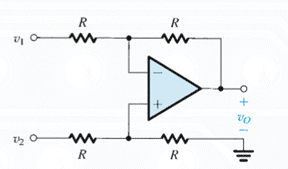
a) v0 = v1 + v2
b) v0 = v2 – v1
c) v0 = v1 – v2
d) v0 = -v1 – v2
Answer: b
Explanation: Considering the fact that the potential at the input terminals are identical and proceeding we obtain the given result.
24. For the difference amplifier shown below, let all the resistors be 10kΩ ± x%. The expression for the worst-case common-mode gain is

a) x / 50
b) x / 100
c) 2x / (100 – x)
d) 2x / (100 + x)
Answer: d
Explanation: None.
25. Determine Ad and Ac for the given circuit.
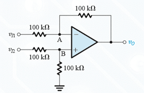
a) Ac = 0 and Ad = 1
b) Ac ≠ 0 and Ad = 1
c) Ac = 0 and Ad ≠ 1
d) Ac ≠ 0 and Ad ≠
Answer: a
Explanation: Consider the fact that the potential at the input terminals are identical and obtain the values of V1 and V2. Thus obtain the value of Vd and Vc.
26. Determine the voltage gain for the given circuit known that R1 = R3 = 10kΩ abd R2 = R4 = 100kΩ.
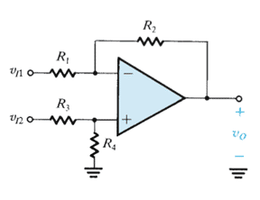
a) 1
b) 10
c) 100
d) 1000
Answer: b
Explanation: Voltage gain is 100/10.
For further doubts and queries ask your question at the bottom of this form else contact us at:7038604912
Prepare For Your Placements: https://lastmomenttuitions.com/courses/placement-preparation/
![]()
/ Youtube Channel: https://www.youtube.com/channel/UCGFNZxMqKLsqWERX_N2f08Q
Follow For Latest Updates, Study Tips & More Content!
Not a member yet? Register now
Are you a member? Login now