Get Latest Exam Updates, Free Study materials and Tips


1.Lead is a metallic crystal having a _______ structure.
a) FCC
b) BCC
c) HCP
d) TCP
Answer: a
Explanation: Crystalline solids are classified as either metallic or non-metallic. Pb, along with Cu, Ag, Al, and Ni, has a face-centered cubic structure.
2.Which of the following has a HCP crystal structure?
a) W
b) Mo
c) Cr
d) Zr
Answer: d
Explanation: Crystalline solids are classified as either metallic or non-metallic. W, Mo, and Cr are examples of the body-centered cubic structure of crystals. The HCP structure is found in Mg, Zn, Ti, Cd, Zr, and others.
3.Amorphous solids have _______ structure.
a) Regular
b) Linear
c) Irregular
d) Dendritic
Answer: c
Explanation: Materials in which the molecule is the basic structural solid and has an irregular structure is known as amorphous solid. Crystalline solids, on the other hand, usually are arranged in a regular manner.
4.At ________ iron changes its BCC structure to FCC.
a) 308oC
b) 568oC
c) 771oC
d) 906oC
Answer: d
Explanation: Similar to metallic crystals, a few non-metallic crystals also change form due to temperature and pressure differences. This process is termed as polymorphism. Iron changes from BCC at room temperature to FCC form at 906oC.
5.At room temperature, tin is formed into _________
a) Gray tin
b) White tin
c) Red tin
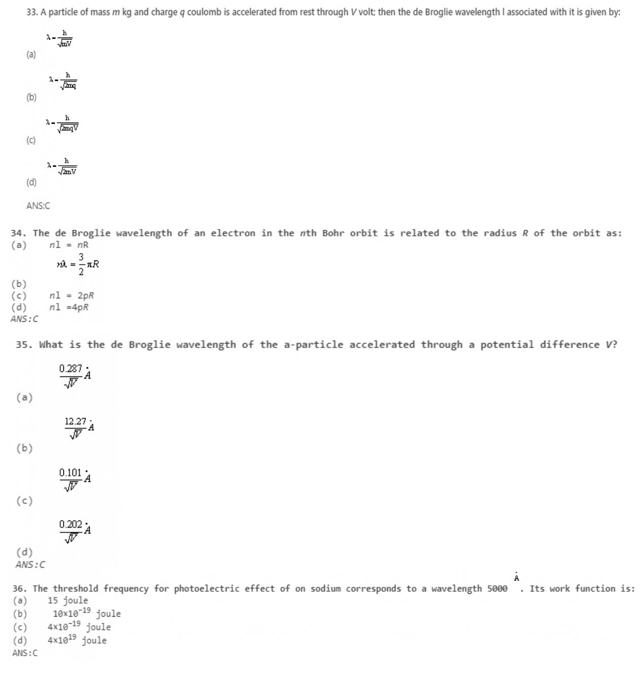
d) Yellow tin
Answer: b
Explanation: Similar to metallic crystals, a few non-metallic crystals also change form due to temperature and pressure differences. Tin crystallizes in a non-metallic diamond structure (gray tin) at low temperatures. At room temperature, it forms a metallic structure (white tin).
7.Which of the following is not an amorphous material?
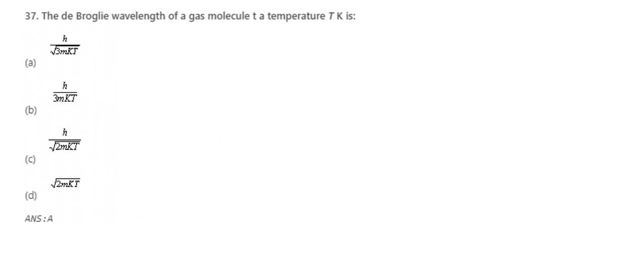
a) Glass
b) Plastics
c) Lead
d) Rubbers
Answer: c
Explanation: Materials in which the molecule is the basic structural solid and has an irregular structure are known as amorphous solid. Most amorphous materials are polymers such as plastics and rubbers. The most common amorphous material is glass.
8.The crystal lattice has a _________ arrangement.
a) One-dimensional
b) Two-dimensional
c) Three-dimensional
d) Four-dimensional
Answer: c
Explanation: Lattice is defined as the regular geometrical arrangement of points in crystal space. Space or crystal lattice is a three-dimensional network of imaginary lines connecting the atoms.
9.The smallest portion of the lattice is known as __________
a) Lattice structure
b) Lattice point
c) Bravais crystal
d) Unit cell
Answer: d
Explanation: Lattice is defined as the regular geometrical arrangement of points in crystal space. The unit cell is the smallest portion of the lattice, which when repeated in all directions gives rise to a lattice structure.
10.Bravais lattice consists of __________ space lattices.
a) Eleven
b) Twelve
c) Thirteen
d) Fourteen
Answer: d
Explanation: There are fourteen ways in which points can be arranged in a space so that each has identical surroundings. These fourteen space lattices constitute the Bravais space lattices.
12.The axial relationship of a monoclinic crystal system is given as ___________
a) a = b = c
b) a = b ≠ c
c) a ≠ b = c
d) a ≠ b ≠ c
Answer: d
Explanation: The crystal system is a format by which crystal structures are classified. Each crystal system is defined by the relationship between edge lengths a, b, and c. For monoclinic, orthorhombic, and triclinic systems, the axial relationship is given by a ≠ b ≠ c.
13.The axial relationship of a rhombohedral crystal system is given as ___________
a) a = b = c
b) a = b ≠ c
c) a ≠ b = c
d) a ≠ b ≠ c
Answer: a
Explanation: The crystal system is a format by which crystal structures are classified. Each crystal system is defined by the relationship between edge lengths a, b, and c. For cubic and rhombohedral systems, the axial relationship is given by a = b = c.
14.The interracial angles of a hexagonal crystal system are given by __________
a) α = β = ϒ = 90o
b) α = β = 90o ϒ = 120o
c) α = β = ϒ ≠ 90o
d) α ≠ β ≠ ϒ ≠ 90o
Answer: b
Explanation: The crystal system is a system by which crystal structures are classified. Each crystal system is defined by the relationship between edge lengths a, b, and c and interaxial angles α, β, and ϒ. For hexagonal system, the interaxial angles are given by α = β = 90o ϒ = 120o.
15.The interracial angles of a triclinic crystal system are given by __________
a) α = β = ϒ = 90o
b) α = β = 90o ϒ = 120o
c) α = β = ϒ ≠ 90o
d) α ≠ β ≠ ϒ ≠ 90o
Answer: d
Explanation: The crystal system is a system by which crystal structures are classified. Each crystal system is defined by the relationship between edge lengths a, b, and c and interaxial angles α, β, and ϒ. For the triclinic system, the interaxial angles are given by α ≠ β ≠ ϒ ≠ 90o.
16.What is the coordination number of a simple cubic structure?
a) 6
b) 8
c) 10
d) 12
Answer: a
Explanation: Coordination number is defined as the number of nearest neighboring atoms in crystals. The coordination number for the simple cubic structure is 6, whereas it is 8 and 12 for BCC and FCC respectively.
17.What is the atomic packing factor of BCC structure?
a) 0.54
b) 0.68
c) 0.74
d) 0.96
Answer: b
Explanation: The density of packing in a crystal is determined using the atomic packing factor (APF). The APF of FCC and HCP structures is 0.74, and 0.54 for simple cubic structure, whereas it is 0.68 for BCC structure.
18.Allotropes differ in which of the following properties:
a) Atomic Number
b) Atomic Mass
c) Crystal Structure
d) Electronegativity
Answer: c
Explanation: Allotropes are different crystalline structures of the same element. Hence, they have the same atomic number, atomic mass and electronegativity. For e.g., graphite and diamond are allotropes of carbon.
19.Co-ordination number of a crystalline solid is:
a) Number of particles in the unit cell
b) Number of nearest neighbours of a particle
c) Number of octahedral voids in a unit cell
d) Number of tetrahedral voids in a unit cell
Answer: b
Explanation: Coordination number of a crystal structure is the number of particles with which a given particle is in direct contact.
20.Packing efficiency of a crystal structure is the ratio of:
a) Volume occupied by particles to the total volume of the unit cell
b) Volume occupied by particles to that by voids
c) Total volume of the unit cell to the volume occupied by particles
d) Volume occupied by voids to that by particles
Answer: a
Explanation: Packing efficiency represents the fraction of the unit cell volume that is utilized to hold the particles.
21.HCP and BCC are called close-packed structures. Close packed structures have:
a) Highest packing efficiency
b) Highest void fraction
c) Highest density
d) All of the mentioned
Answer: a
Explanation: Due to the largest number of particles in a unit cell, close-packed structures have the highest packing efficiency and hence, lest void fraction. Density is NOT a property of the crystal structure but the substance and depends also on molar mass.
22.Which of the following is a property of amorphous solids?
a) Sharp melting point
b) Isotropy
c) Long range order
d) Definite heat of fusion
Answer: b
Explanation: Due to irregularity in structure, the average of physical properties like density, thermal and electrical conductivity etc. is same along any direction for a particular amorphous solid.
23.Which of the following is a crystalline solid?
a) Copper wire
b) Glass bottle
c) Polythene bag
d) Rubber ball
Answer: a
Explanation: Copper wires are made of crystalline copper. In fact, most metallic objects are crystalline. However, research for the large-scale production of amorphous metals is in progress.
24.The smallest portion of a crystal which when repeated in different directions generates the entire crystal is called:
a) Lattice points
b) Crystal lattice
c) Unit cell
d) None of the mentioned
Answer: c
Explanation: Unit cell is the smallest unit of a crystal which repeats itself to generate the crystal. Lattice point represents the centres of atoms in a unit cell. Crystal lattice refers to the entire structure of a crystalline solid.
25.Which of the following is not a property of metal glass?
a) Transparent
b) Poor thermal conductivity
c) High magnetic susceptibility
d) None of the mentioned
Answer: a
Explanation: Metal glass is a form of metal which like glass, is amorphous but not transparent. Most of the metal glasses are alloys, having high yield strength and high elastic strain limits. High magnetic susceptibility, low coercivity and comparatively higher electrical resistance than their crystalline counterparts make them an ideal material for power transformers.
26.Grain boundaries are one of the causes of corrosion of metals?
a) True
b) False
Answer: a
Explanation: Grain boundaries are the regions that separate two grains in polycrystalline metallic solids. The absence of properly defined structure results in residual stresses. Hence, grain boundaries are the weak spots in the structure and are often the site of a fracture.
27.The correct expression for Bragg’s law is nλ = ___________
a) dsinθ
b) dcosθ
c) 2dsinθ
d) 2dcosθ
Answer: c
Explanation: Bragg’s law gives us the relation between the wavelength of the incident X-ray and the angle of incidence. The expression is: nλ = 2dsinθ.
29.When X-ray are incident on an atom, they make an electronic cloud move.
a) True
b) False
Answer: a
Explanation: X-ray is an electromagnetic wave. So, just like any other electromagnetic wave, when X-ray is incident on an atom, it makes the electronic cloud around that atom to move.
30.The scattering of waves in Bragg’s law experiment is due to __________
a) Einstein’s scattering
b) Rayleigh scattering
c) Newton scattering
d) Inelastic scattering
Answer: b
Explanation: In Bragg’s law experiment, the phenomenon is observed due to the Rayleigh scattering, i.e., the movement of charges is re-radiated with the wave of same frequency.
31.Bragg’s law is a special case of Laue diffraction.
a) True
b) False
Answer: a
Explanation: Laue diffraction is the one used in X-ray crystallography. Bragg’s law is only a special case of Laue diffraction with the condition that the incident angle be equal to scattering angle and the wavelength is integer times the path difference.
32.Bragg’s law was proposed in __________
a) 1903
b) 1913
c) 1893
d) 1853
Answer: b
Explanation: Lawrence Bragg and William Henry Bragg proposed Bragg’s law in 1913. It was based on the fact that surprising patterns are observed when the X-rays are reflected by a crystalline solid.
33.If the angle of incidence is 30°, then the wavelength for first-order spectrum is equal to __________
a) d
b) 2d
c) d/2
d) d/3
Answer: a
Explanation: We know, nλ = 2dsinθ.
As, θ = 30° and n = 1, we get
λ = d.
1.Which states get filled in the conduction band when the donor-type impurity is added to a crystal?
a) Na
b) Nd
c) N
d) P
Answer: b
Explanation: When the donor-type impurity is added to a crystal, first Nd states get filled because it is of the highest energy.
2.When the temperature of either n-type or p-type increases, determine the movement of the position of the Fermi energy level?
a) Towards up of energy gap
b) Towards down of energy gap
c) Towards centre of energy gap
d) Towards out of page
Answer: c
Explanation: whenever the temperature increases, the Fermi energy level tends to move at the centre of the energy gap.
3.Is it true, when the temperature rises, the electrons in the conduction band becomes greater than the donor atoms?
a) True
b) False
Answer: a
Explanation: When the temperature increases, there is an increase in the electron-hole pairs and all the donor atoms get ionized, so now the thermally generated electrons will be greater than the donor atoms.
3.If excess charge carriers are created in the semiconductor then the new Fermi level is known as Quasi-Fermi level. Is it true?
a) True
b) False
Answer: a
Explanation: Quasi-fermi level is defined as the change in the level of the Fermi level when the excess chare carriers are added to the semiconductor.
4.Ef lies in the middle of the energy level indicates the unequal concentration of the holes and the electrons?
a) True
b) False
Answer: b
Explanation: When the Ef is in the middle of the energy level, it indicates the equal concentration of the holes and electrons.
5.In a P-N Junction, the depletion region is reduced when _________
a) P side is connected to the negative side of the terminal
b) P side is connected to the positive side of the terminal
c) N side is connected to the positive side of the terminal
d) Never reduced
Answer: b
Explanation: When the P-side of a P-N junction is connected to the positive terminal of a battery, the junction is forward biased and hence the depletion region reduces.
6.The voltage at which forward bias current increases rapidly is called as ___________
a) Breakdown Voltage
b) Forward Voltage
c) Knee Voltage
d) Voltage barrier
Answer: c
Explanation: Till the knee voltage, the current in a semiconductor increases slowly. After Knee voltage, the current increases rapidly for a small change in the voltage.
7.The Knee Voltage for germanium is _________
a) 0.1 V
b) 0.3 V
c) 0.7 V
d) 1.4 V
Answer: b
Explanation: Knee voltage or the threshold voltage is the point after which the current increases rapidly. For germanium, it is about 0.3 V while for silicon it is 0.7 V.
8.The resistance of the semiconductor decreases in forward biased.
a) True
b) False
Answer: a
Explanation: When a P-N Junction diode is forward biased, the thickness of the depletion region becomes negligibly small. Thus, the resistance of the semiconductor decreases.
9.The current produced in reverse-bias is called as __________
a) Reverse Current
b) Breakdown Current
c) Negative Current
d) Leakage Current
Answer: d
Explanation: When the diode is reverse biased, the reverse bias voltage produces an extremely small current, about a few micro amperes. This is called leakage current.
10.Which diode is designed to work under breakdown region?
a) Photodiode
b) Light Emitting Diode
c) Solar Cell
d) Zener diode
Answer: d
Explanation: Zener Diode is designed specifically to operate in the breakdown region. It is mostly used as a voltage regulator in various circuits.
12.The leakage current is measured in ________
a) A
b) mA
c) μA
d) nA
Answer: c
Explanation: As in the reverse current, the resistance increases, the current produced is extremely low. And hence, it is measured in microamperes.
13.How does a semiconductor behave at absolute zero?
a) Conductor
b) Insulator
c) Semiconductor
d) Protection device
Answer: b
Explanation: A semiconductor is a solid which has the energy band similar to that of the insulator. It acts as an insulator at absolute zero.
14.Semiconductor acts as an insulator in the presence of impurities.
a) True
b) False
Answer: b
Explanation: When the temperature is raised or when an impurity is added, their conductivity increases. Conductivity is inversely proportional to temperature.
15.How is the resistance of semiconductor classified?
a) High resistance
b) Positive temperature co-efficient
c) Negative temperature co-efficient
d) Low resistance
Answer: c
Explanation: Semiconductors have negative temperature co-efficient. The reason for this is, when the temperature is increased, a large number of charge carriers are produced due to the breaking of covalent bonds and hence these electrons move freely and gives rise to conductivity.
16.What are the charge carriers in semiconductors?
a) Electrons and holes
b) Electrons
c) Holes
d) Charges
Answer: a
Explanation: In conductors, electrons are charge carriers. But in semiconductors, both electrons and holes are charge carriers and will take part in conduction.
17.Which of the following is known as indirect band gap semiconductors?
a) Germanium
b) Nickel
c) Platinum
d) Carbon
Answer: a
Explanation: The elemental semiconductor is made up of a single element from the fourth column elements such as Germanium. Here recombination takes place takes place via traps. It is called indirect band gap semiconductors.
19.Compound semiconductors are also known as direct band gap semiconductors.
a) True
b) False
Answer: a
Explanation: In compound semiconductors, recombination takes place directly and its energy difference is emitted in the form of photons in the visible or infrared range. Hence the compound semiconductors are also known as direct band gap semiconductors.
20.How are charge carriers produced in intrinsic semiconductors?
a) By pure atoms
b) By electrons
c) By impure atoms
d) By holes
Answer: c
Explanation: Impure semiconductors in which the charge carriers are produced due to impurity atoms are called extrinsic semiconductors. They are obtained by doping an intrinsic semiconductor with impurity atoms.
22.What type of material is obtained when an intrinsic semiconductor is doped with trivalent impurity?
a) Extrinsic semiconductor
b) Insulator
c) N-type semiconductor
d) P-type semiconductor
Answer: d
Explanation: P-type semiconductor is obtained by doping an intrinsic semiconductor with trivalent impurity.
23.A light emitting diode is _________
a) Heavily doped
b) Lightly doped
c) Intrinsic semiconductor
d) Zener diode
Answer: a
Explanation: A light emitting diode, LED, is heavily doped. It works under forward biased conditions. When the electrons recombine with holes, the energy released in the form of photons causes the production of light.
24.Which of the following materials can be used to produce infrared LED?
a) Si
b) GaAs
c) CdS
d) PbS
Answer: b
Explanation: GaAs has an energy band gap of 1.4 eV. It can be used to produce infrared LED. Various other combinations can be used to produce LED of different colors.
25.The reverse breakdown voltage of LED is very low.
a) True
b) False
Answer: a
Explanation: The reverse breakdown voltages of LEDs are very low, typically around 5 V. So, if access voltage is provided, they will get fused.
26.What should be the band gap of the semiconductors to be used as LED?
a) 0.5 eV
b) 1 eV
c) 1.5 eV
d) 1.8 eV
Answer: d
Explanation: Semiconductors with band gap close to 1.8 eV are ideal materials for LED. They are made with semiconductors like GaAs, GaAsP etc.
27.What should be the biasing of the LED?
a) Forward bias
b) Reverse bias
c) Forward bias than Reverse bias
d) No biasing required
Answer: a
Explanation: The LED works when the p-n junction is forward biased i.e., the p- side is connected to the positive terminal and n-side to the negative terminal.
28.Increase in the forward current always increases the intensity of an LED.
a) True
b) False
Answer: b
Explanation: As the forward current is increased for an LED, the intensity of the light increases up to a certain maximum value. After that, the intensity starts decreasing.
29.Which process of the Electron-hole pair is responsible for emitting of light?
a) Generation
b) Movement
c) Recombination
d) Diffusion
Answer: c
Explanation: When the recombination of electrons with holes takes place, the energy is released in the form of photon. This photon is responsible for the emission of light.
30.What is the bandwidth of the emitted light in an LED?
a) 1 nm to 10 nm
b) 10 nm to 50 nm
c) 50 nm to 100 nm
d) 100 nm to 500 nm
Answer: b
Explanation: The bandwidth of the emitted light is 10 nm to 50 nm. Thus, the emitted light is nearly (but not exactly) monochromatic.
33.The term photo voltaic comes from ________
a) Spanish
b) Greek
c) German
d) English
Answer: b
Explanation: The term photo voltaic comes from Greek word phos means light. The volt is the unit of emf which was named after inventor of the battery.
34.The volt is the units of emf that was named after its inventor _________
a) Alessandro volta
b) Alxender volta
c) Alexa volta
d) Alexandro volta
Answer: a
Explanation: The volt is the units of that was named after its inventor Alessandro volta. He is an Italian physicist. The term photo voltaic comes from Greek.
35.The term photo voltaic is in use since _________
a) 1840
b) 1844
c) 1849
d) 1850
Answer: c
Explanation: The term photo voltaic is in use since 1849. Photo voltaic is a field related to practical application of photo voltaic cells.
36.When the source of light is not sun light then the photo voltaic cell is used as ____________
a) Photo diode
b) Photo voltaic cell
c) Photo detector
d) Photo transmitter
Answer: c
Explanation: When the source of light is not the sun light then the photo voltaic cell is used as the photo detector. The example of the photo detector is the infra-red detectors.
38.The amount of photo generated current increases slightly with an increase in _________
a) Temperature
b) Photons
c) Diode current
d) Shunt current
Answer: a
Explanation: The amount of the photo generated current is slightly increased due to an increase in the temperature. If the photo generated current increases then the output current increases.
39.Solar cells are made from bulk materials that are cut into wafer of _________ thickness.
a) 120-180μm
b) 120-220μm
c) 180-220μm
d) 180-240μm
Answer: d
Explanation: Solar cells are made from the bulk materials that are cut into wafers of thickness 180-240μm. Many currently available cells are cut into wafers.
40.__________ is one of the most important materials is also known as solar grade silicon.
a) Crushed silicon
b) Crystalline silicon
c) Powdered silicon
d) Silicon
Answer: b
Explanation: The crystalline silicon is one of the most important materials that are also called as solar grade silicon. The mono crystalline, poly crystalline silicon and ribbon silicon are the other types of silicon that are used.
42.__________ is a direct band gap material.
a) Copper Indium Gallium Selenide
b) Copper Selenide
c) Copper Gallium Telluride
d) Copper Indium Gallium Diselenide
Answer: a
Explanation: Copper Indium Gallium Selenide is a direct band gap material. It has the highest efficiency among the film materials. The efficiency is about 20%.
43.Dye-sensitized solar cells are made from ________ organic dye.
a) Ruthium melallo
b) Aniline
c) Safranine
d) Induline
Answer: a
Explanation: Dye-sensitized solar cells are made from Ruthium melallo organic dye in the form of mono layer of light absorbing material and mesoporous layer of nano particles.
44.Quantum dot solar cells are based on _______
a) Gratzel cell
b) Solar cell
c) Voltaic cell
d) Galvanic cell
Answer: a
Explanation: Quantum dot solar cells are based on the Gratzel cell or dye sensitized solar cell. In dye-sensitized solar cell the nano particulate is titanium dioxide that amplifies the surface area greatly.
45.The quantum dot used are _______
a) Cds
b) CdTe
c) PbO
d) GaAs
Answer: a
Explanation: The quantum dot used is generally is Cds. The other quantum dots that are used is cadmium selluroide, PbS etc.
46.Organic polymer solar cells are made from Polyphenylene.
a) True
b) False
Answer: a
Explanation: Organic polymer solar cells are made from organic semi conductors. Some of them are Polyphenylene, Vinylene, Carbon fullerenes.
47.Zener diode is designed to specifically work in which region without getting damaged?
a) Active region
b) Breakdown region
c) Forward bias
d) Reverse bias
Answer: b
Explanation: The Zener diode is a specifically designed diode to operate in the breakdown region without getting damaged. Because of this characteristic, it can be used as a constant-voltage device.
49.When the reverse voltage across the Zener diode is increased _____________
a) The value of saturation current increases
b) No effect
c) The value of cut-off potential increases
d) The value of cut-off potential decreases
Answer: c
Explanation: As the frequency of the incident radiation increases, the kinetic energies of the emitted electron are higher and therefore require more repulsive force to be applied to stop them.
The value of saturation current increases, as the intensity of the incident radiation, increases.
50.The value of cut-off potential decreases, as the frequency decreases.
Zener Diode is mostly used as ____________
a) Half-wave rectifier
b) Full-wave rectifier
c) Voltage Regulator
d) LED
Answer: c
Explanation: The Zener diode, once in the breakdown region, keeps the voltage in the circuit to which it is connected as constant. Thus it is widely used as a voltage regulator.
51.In normal junctions, the breakdown is same as Zener breakdown.
a) True
b) False
Answer: b
Explanation: In normal p-n unction diodes, the breakdown takes place by avalanche breakdown which is different than the Zener breakdown. Zener diode is specifically made to operate in that region.
52.The depletion region of the Zener diode is ____________
a) Thick
b) Normal
c) Very Thin
d) Very thick
Answer: c
Explanation: Zener diode is fabricated by heavily doping both p- and n-sides of the junction, which results in an extremely thin depletion region.
1. Which of the following does not show any interference pattern?
a) Soap bubble
b) Excessively thin film
c) A thick film
d) Wedge Shaped film
Answer: b
Explanation: An excessively thin film shows no interference pattern because in that case, as the thickness of the film is negligible, the path difference, Δ, between the two reflected rays turns out to be λ/2 which is the condition of minima. Hence, the pattern is not observed.
The interference pattern is observed in the soap bubble, thick film, and wedge-shaped film.
2. The main principle used in Interference is _____________
a) Heisenberg’s Uncertainty Principle
b) Superposition Principle
c) Quantum Mechanics
d) Fermi Principle
Answer: b
Explanation: Superposition principle is the basic principle used in the interference of light. When the incoming light waves superimpose constructively, the intensity increases while when they add destructively, it decreases.
3. When Two waves of same amplitude add constructively, the intensity becomes _____________
a) Double
b) Half
c) Four Times
d) One-Fourth
Answer: c
Explanation: As we know, I ∝ A2. Thus, as the two waves add constructively, their amplitude becomes twice and hence the intensity becomes four times.
4. The shape of the fringes observed in interference is ____________
a) Straight
b) Circular
c) Hyperbolic
d) Elliptical
Answer: c
Explanation: The fringes observed in an interference pattern are hyperbolic in shape. When the distance between the slits and the screen is large, they appear almost straight.
5. If instead of monochromatic light white light is used for interference of light, what would be the change in the observation?
a) The pattern will not be visible
b) The shape of the pattern will change from hyperbolic to circular
c) Colored fringes will be observed with a white bright fringe at the center
d) The bright and dark fringes will change position
Answer: c
Explanation: When white light is used instead of monochromatic light, all the seven constituent colors produce their interference pattern. At the center of the screen, all the wavelengths meet in phase and, therefore, a white bright fringe is formed. Then the next fringe will be formed due to violet color as the wavelength is shortest for violet color. This will be followed by indigo, blue till red color.
6. Zero order fringe can be identified using ____________
a) White light
b) Yellow light
c) Achromatic light
d) Monochromatic light
Answer: a
Explanation: When the white light is used, the central fringe is white in color while the rest are colored. Thus, the central fringe can be identified using white light.
7. Interference is observed only when the phase difference between the two waves is zero.
a) True
b) False
Answer: b
Explanation: For interference pattern, the phase difference between the two rays must be constant. It is not necessary that the phase difference between the two rays has to be zero.
8. The shape of the pattern depends on the ____________
a) Distance between the slits
b) Distance between the slits and the screen
c) Wavelength of light
d) Shape of the slit
Answer: d
Explanation: The shape of the interference pattern observed depends on the shape of the slits. If the shape of the slits changes, the shape of the fringes changes.
9. A thin sheet of refractive index 1.5 and thickness 1 cm is placed in the path of light. What is the path difference observed?
a) 0.003 m
b) 0.004 m
c) 0.005 m
d) 0.006 m
Answer: c
Explanation: AS we know, the path difference introduced by the sheet = (μ – 1) t, where t is the thickness of the sheet.
Here, μ = 1.5 and t = 0.01 m
Therefore, Δx = 0.5 X 0.01 m
= 0.005 m.
10. According to stoke’s law, the expression for maxima is: 2μtcosr = ____________
a) nλ
b) 2nλ
c) (2n + 1) λ/2
d) (n + 1) λ/2
Answer: c
Explanation: Stoke’s relation states that when a light ray is incident on the interface of the optically denser medium, then the reflected wave suffers a phase change of π. Thus, for maxima 2μtcosr = (2n + 1) λ/2 and for minima 2μtcosr = nλ.
12. When a thin plate of refractive index 1.5 is placed in the path of one of interfering beams of Michaelson Interferometer, a shift of 30 fringes is observed. If the thickness of plate is 0.018 mm, the wavelength of the used light is ___________
a) 4000 Å
b) 5000 Å
c) 6000 Å
d) 7000 Å
Answer: c
Explanation: Here, μ = 1.5, n = 30, t = 1.8 X 10⁻⁵ m
Path difference due to the glass plate = 2(μ – 1) t
2(μ – 1) t = nλ
λ = 2(μ – 1) t/n
= 2 X 0.5 X 1.8 X 10-5/30
= 6000 Å.
13. A thin layer of colorless oil is spread over water in a container (μ = 1.4). If the light of wavelength 640 nm is absent in the reflected light, what is the minimum thickness of oil layer?
a) 179.6 nm
b) 198.3 nm
c) 207.6 nm
d) 214.3 nm
Answer: d
Explanation: Let t be the thickness of the oil layer spread on water.
For minima, 2μtcosr = nλ
For minimum thickness, we take n = 1.
Therefore, tmin = λ/2μ
= 600 nm/2.8
= 214.3 nm.
14. In Newton’s ring experiment, the diameter of the 10th ring changes from 1.40 to 1.23 cm when a liquid is introduced between the lens and glass plate. What is the refractive index of the liquid?
a) 1.05
b) 1.15
c) 1.25
d) 1.35
Answer: c
Explanation: We know, Dn2 = 4nλR/μ
Without liquid in air, μ = 1, D102 = 40λR
With liquid, D102’ = 40λR/μ
Dividing both we get, μ = D102 D102’
= {1.40/1.27}2
= 1.25.
15. In Young’s Double Slit Experiment, if instead of monochromatic light white light is used, what would be the observation?
a) The pattern will not be visible
b) The shape of the pattern will change from hyperbolic to circular
c) Colored fringes will be observed with a white bright fringe at the center
d) The bright and dark fringes will change position
Answer: c
Explanation: When white light is used instead of monochromatic light in Young’s Double Slit experiment, all the seven constituent colors produce their interference pattern. At the center of the screen, all the wavelengths meet in phase and, therefore, a white bright fringe is formed. Then the next fringe will be formed due to violet color as the wavelength is shortest for violet color. This will be followed by indigo, blue till red color.
17. What kind of sources are required for Young’s Double Slit experiment?
a) Coherent
b) Incoherent
c) Intense
d) Bright
Answer: a
Explanation: For the interference pattern to be visible, coherent sources are required. If the sources are coherent, only then would there be constructive interference.
18. If the distance between the two slits is doubled, the fringe width _________
a) Doubles
b) Halves
c) Four-times
d) Remains same
Answer: b
Explanation: The fringe width is inversely proportional to the distance between the two slits. As the distance between the slits doubles, the fringe width becomes half of its original value.
19. What change is observed when the whole pattern is immersed in water?
a) Fringe width decreases
b) Fringe width increases
c) Colored fringes
d) The bright and dark fringes will change position
Answer: a
Explanation: When the whole apparatus of Young’s Double slit experiment is immersed in water, the only change is the pattern shrinks a bit. The width of the fringes decreases, as an external path difference is present because of the water.
20. In YDS, the width of the fringes obtained from a light of wavelength 500 nm is 3.6 mm. What is the fringe width id the apparatus is immersed in a liquid of refractive index 1.2?
a) 2 mm
b) 2.6 mm
c) 3 mm
d) 3.2 mm
Answer: c
Explanation: AS we know, Fringe width, β = λD/d, where D is the distance between the slits and the screen and d is the distance between the slits.
Now, β’ = λ’D/d
β’/ β = λ’/λ
β’ = β/μ
= 3.6 mm/1.2
= 3 mm.
22. In a Young’s double slit experiment, the distance between the two slits is 0.5 mm and the distance between the screen and the slits is 1 m. When a light of wavelength 500 nm is incident on the slits, what would be distance between the two second bright fringes?
a) 1 mm
b) 2 mm
c) 3 mm
d) 4 mm
Answer: b
Explanation: As we know, β = λD/d. In this question, we need to find 2 X β.
Here, d = 0.5 mm and D = 1 m
Therefore, β = 500 nm / 0.5 mm
= 1 mm
Now, Separation between the second bright fringe on both sides of the central maxima = 2 X 1 mm
= 2 mm.
23. A thin sheet of refractive index 1.25 and thickness 0.5 cm is placed in the path of light from one source in the Young’s double slit experiment. What is the path difference observed?
a) 1.25 mm
b) 2.5 mm
c) 2.78 mm
d) 3.25 mm
Answer: a
Explanation: As we know, the path difference introduced by the sheet = (μ – 1) t, where t is the thickness of the sheet.
Here, μ = 1.5 and t = 0.01 m
Therefore, Δx = 0.25 X 0.005 m
= 0.0012 m
= 1.25 mm.
24. A Young’s double slit apparatus is immersed in a liquid of refractive index 1.25. What is the ratio of the fringe width in air and liquid?
a) 1: 2
b) 4: 5
c) 5: 4
d) 2: 1
Answer: c
Explanation: In air, β = λaD/d
In liquid, β’ = λlD/d
Now, β: β’ = λa: λl
= μ : 1
= 5 : 4.
25. Two narrow and parallel slits 0.08 cm apart are illuminated by a light of frequency 6 X 10¹¹ kHz. At what distance from the slits should the screen be placed to obtain fringe width of 0.6 mm?
a) 0.98 m
b) 1.06 m
c) 1.28 m
d) 1.74 m
Answer: c
Explanation: Here, d = 0.08 cm = 8 X 10⁻⁴ m, β = 0.6mm = 6 X 10⁻⁴ m
λ = c/v
= 3 X 10⁸/8 X 1014
= 3.75 X 10⁻⁷ m
D = βd/λ
= 1.28 m.
26. When a plate of thickness 0.05 mm is placed in the path of a Michaelson Interferometer, a shift of 100 fringes is observed for a light of wavelength 5000 Å. What is the refractive index of the plate?
a) 1
b) 1.5
c) 2
d) 2.5
Answer: b
Explanation: We know, μ = nλ/2t + 1
Here, λ = 5000 Å = 5 X 10⁻⁷ m, n = 100, t = 0.05 mm = 5 X 10⁻⁵ m
Therefore, μ = 100 X 5 X 10-7/2 X 5 X 10-5 + 1
μ = 1.5.
28. In Young’s Double Slit experiment, the angular width of the fringe is 0.1o. If the light used has a wavelength of 600 nm, what is the spacing between the slits?
a) 0.17 mm
b) 0.23 mm
c) 0.34 mm
d) 0.49 mm
Answer: c
Explanation: Now, as we know, β = λD/d
βθ = θn+1 – θn = β/D
βθ = λ/d
Here, λ = 6 X 10⁻⁷ m and βθ = 0.1 X π/180 radians
Therefore, d = 6 X 10-7 m X 180 = 0.1 X π
= 0.344 mm.
1.A solid that offers no _________ passage of electricity is called super conductors.
a) Conductance
b) Inductance
c) Resistance
d) Impedance
Answer: c
Explanation: A solid that offers no resistance passage of electricity is called super conductors. They are very good conductors of electricity.
2.The phenomena of super conductors was first discovered by ___________
a) Kammerlingh Onnes
b) Neils bohr
c) Richard Smalley
d) Otto lehman
Answer: a
Explanation: The phenomena of super conductors were first discovered by Kammerlingh Onnes. Neils bohr given about atomic structure. Richard Smalley discovered the fullerene by laser ablation method. Otto lehman coined the name liquid crystal.
3.Super conductors are discovered in the year _______
a) 1900
b) 1991
c) 1911
d) 1905
Answer: c
Explanation: Super conductors are discovered in the year 1911 by Kammerlingh Onnes. He is a Dutch physicist. When he was measuring the resistivity of the mercury below 4.2K he found the super conductors.
4.The earliest superconductors to be studied elaborately is ________
a) Niobium alloy
b) Copper alloys
c) Steel alloys
d) Iron alloy
Answer: a
Explanation: The earliest superconductors to be studied elaborately are niobium alloy. The super conductivity can be understood with the help of quantum physics.
5.The shifting of electrons in super conductors is prevented by _________
a) Quantum effect
b) Threshold energy level
c) Energy barrier
d) Orbitals
Answer: a
Explanation: The shifting of electrons in super conductors is prevented by quantum energy. Electrons in normal metals shift from one energy level to another.
6.The electrons head in ___________ direction.
a) Same
b) Different
c) Opposite to one another
d) Random
Answer: a
Explanation: The electrons head in same direction and continue to carry current endlessly. As they are in same direction, they do not collide with each other.
7.The normal metal passes into super conducting state at ___________
a) High temperature
b) Low temperature
c) Critical temperature
d) No temperature
Answer: c
Explanation: The normal metal passes into super conducting state at critical temperature. Most of the metals act as super conductors at low temperatures.
8.Based on magnetic response super conductors are of __________ types.
a) 1
b) 2
c) 3
d) 4
Answer: b
Explanation: Based on the magnetic response super conductors are of two types. They are ideal super conductors or hard super conductors.
9.Ideal super conductors completely become __________ at super conducting state.
a) Diamagnetic
b) Ferro magnetic
c) Ferri magnetic
d) Para magnetic
Answer: a
Explanation: Ideal super conductors become diamagnetic at super conducting state. The permeability is less than that of permeability in Vaccum.
10.The ideal super conductors exhibit __________
a) Meissner effect
b) Mesmeric effect
c) Mesomeric effect
d) Monomeric effect
Answer: a
Explanation: The ideal super conductors exhibit meissner effect. The expulsion of magnetic flux from the interior of a piece of super conducting material as the material undergoes transition to super conducting phase.
11.The hard super conductors are those in which the ideal behaviour is seen up to a ________ critical magnetic field.
a) Higher
b) Lower
c) Moderate
d) Zero
Answer: b
Explanation: The hard super conductors are those in which the ideal behaviour is seen up to a lower critical magnetic field beyond which the magnetization gradually changes and attains zero.
12.The constituents of this material that is yttrium, barium and copper are in ____________
a) 1:1:1
b) 1:2:2
c) 1:2:3
d) 1:2:1
Answer: c
Explanation: The constituents of this material that yttrium, barium and copper are in 1:2:3 molar stoichiometric ratios and hence are called as 1:2:3 super conductors.
13.Annealing the homogeneous mixture to room temperature to retain its __________
a) Composition
b) Structure
c) Its properties
d) Composition, structure and its properties
Answer: d
Explanation: Annealing the homogeneous mixture to room temperature to retain its composition, structure and its properties. Heating them to obtain an oxygen deficient super conductors.
14.In superconductivity the conductivity of a material becomes
a.Zero
b.Finite
c.Infinite
d.None of the above
Answer:c
15.In superconductivity, the electrical resistance of material becomes
a.Zero
b.Infinite
c.Finite
d.All of the above
Answer:a
16.The temperature at which conductivity of a material becomes infinite is called
a.Critical temperature
b.Absolute temperature
c.Mean temperature
d.Crystallization temperature
Answer:a
17.In superconductors, the Fermi energy level is
a.Below the ground state
b.Midway between the ground state and first excited state
c.Above first excited state
d.At first excited state
Answer:b
18.The superconducting state is perfectly _____ in nature.
Diamagnetic
Paramagnetic
Ferromagnetic
Ferromagnetic
Answer:a
19.Which of the following are the properties of superconductors?
a.They are diamagnetic in nature
b.They have zero resistivity
c.They have infinite conductivity
d.All of the above
Answer:d
20.The minimum amount of current passed through the body of superconductor in order to destroy the superconductivity is called
a.Induced current
b.Critical current
c.Eddy current
d.Hall current
Answer:b
22.The binding energy for a cooper pair is
a.10^-2 eV
b.10^-4 eV
c.10^-6 eV
d.10^-8 eV
Answer:b
23.There are three important lengths which enter the theory of superconductivity except
London penetration length
Intrinsic coherence length
Normal electron mean free length
Mean path length
(Ans:d)
24.The magnetic lines of force cannot penetrate the body of a superconductor, a phenomenon is known as
a.Isotopic effect
b.BCS theory
c.Meissner effect
d.London theory
Answer:c
25.Which of the following conductor has highest critical temperature?
a.Aluminium
b.Zinc
c.Molybdenium
d.Tin
Answer:d
26.Fermi energy level
a) is the top most filled energy level at 0K temperature
b) is the top most filled energy level at 00C temperature
c) separates valence band and conduction band
d) none of the above
Ans: a and c both
28.Fermi-Dirac statistics explains
(a) how electrons are distributed among different energy levels
(b) the probability of an energy level to be occupied by electrons
(c) the probability of an energy level to be occupied by quantum mechanical particles
(d) how quantum mechanical particles are distributed in different energy
level.
Ans: All are correct
29.Fermi-Dirac (FD) statistics governs
(a) fermions
(b) free electrons
(c) gas molecules
(d) All the above
Ans: a and b
30.In free electron gas theory, electrons
(a) can move anywhere inside the metal.
(b) are considered as a gas.
(c) pairs with holes and become neutral.
(d) All the above.
Ans: a and b
32.Free electron theory gas is applicable to
(a) metals
(b) gas
(c) solids
(d) all the above.
Ans: a and c. a is a more accurate answer
33.Free electron gas theory assumes
(a) electrons are free from Coulomb force
(b) the Coulomb force of repulsion is negligible.
(c) Electrons are free to move anywhere.
(d) All the above.
Ans: b. Electrons are free to move inside the metal only
34.For a semiconductor-based light source, it should be a
(a) direct bandgap semiconductor
(b) indirect direct bandgap semiconductor
(c) either direct bandgap or indirect bandgap
(d) the semiconductor can not be used as a light source
Ans: a
35.In an indirect bandgap semiconductor, a transition between conduction
band and valance band results in
(a) heat
(b) light
(c) both
(d) none of the above.
Ans: a
36.In a direct bandgap semiconductor
(a) The two points of intersection of a vertical line with the E-K curve of
both valance band and conduction band are at the same momentum.
(b) The two points of intersection of a vertical line with the E-K curve of both
valance band and conduction band are having the same wave vector.
(c) The K value of the lowest point of the conduction band is equal to the K
value of highest point of valance band.
(d) The transitions of electrons take place directly.
Ans: All are correct.
37.Which of the following is true?
(a) In an indirect bandgap semiconductor, emission of photons is not
possible
(b) In a direct bandgap semiconductor emission of both light and heat
is possible.
Ans: b. Option a is not true. The emission of photons is possible with less probability.
38.In an indirect bandgap semiconductor, emission of light does not occur
because of the fact that
(a) momentum is not conserved in case of direct transition
(b) electrons are trapped in defects before making the transition.
Ans: a and b
39.Which of the following is an indirect bandgap semiconductor?
(a) silica
(b) germanium
(c) carbon
(d) all the above.
Ans: d
40.Which of the following is a radiative semiconductor
(a) Silica
(b) Gallium Arsenide
(c) Germanium
(d) None of the above
Ans: b. The radiative semiconductor is the one that emits light.
42.The shape of E-K diagram of the conduction band and valance band is
(a) horizontal
(b) vertical
(c) parabolic
(d) none of the above.
Ans: c
43.The curvature of E-K diagram
(a) is higher in conduction band than valance band
(b) is lower in valence band than the conduction band
(c) is negative in the conduction band
(d) b and c
Ans: a and b. Curvature is negative in the valance band.
44.The symbol K in Fermi energy represents
(a) Maxwell-Boltzmann constant
(b) Boltzmann constant
(c) Wave vector
(d) None of the above.
Ans: b. K is a wave vector or propagation constant in the wave function.
45.Hertz is the unit of
(a) frequency of ultrasound
(b) frequency of AC
(c) frequency of waves
(d) all the above.
Ans: d
46.The effective mass of a charge carrier
(a) is directly proportional to the curvature of E-K curve
(b) is inversely proportional to the curvature of E-K curve
(c) is positive near the bottom of the conduction band
(d) is negative near the top of the valance band
Ans: b, c, d. The effective mass may be positive or negative according to the sign of curvature. The curvature may be positive or negative in both the conduction band and the valance band.
47.Electronic bands are formed due to
(a) split-up of energy levels
(b) to satisfy Pauli’s exclusion principle
(c) The shift in energy levels
(d) All the above
Ans: a and b
48.An electronic band is
(a) Any range of energy levels
(b) Energy levels where free electrons exist
(c) A range of energy level is characterized by the existence of
electrons.
(d) All the above.
Ans: c
49.The interaction of different atoms leads to the formation of
(a) electronic band
(b) electronic bond
(c) none of the above
(d) all the above
Ans: a and b
50.A forbidden band
(a) is the one where electrons are forbidden
(b) is the one where energy is forbidden
(c) is not there in between the conduction and valence band in conductors
(d) all the above.
Ans: a and c
52.Dopant for N-type semiconductor
(a) should be a pentavalent impurity
(b) should be a trivalent impurity
(c) either a or b
(d) depends on the number of valance electrons in the host atom
Ans: a
53.Hall voltage is developed due to the
(a) change in the magnetic field
(b) change in the electric field
(c) polarization of charge
(d) none of the above.
Ans: c
54.In the Hall effect, electrons experience
(a) electrostatic force
(b) magnetic force
(c) Lorentz force
(d) all the above
Ans: c
55.The force acting on moving electrons due to a perpendicular magnetic
the field is in the direction
(a) parallel to the magnetic field
(b) perpendicular to the magnetic field and parallel to the direction of electrons
(c) perpendicular to the direction of electrons and parallel to the magnetic field
(d) Opposite to the magnetic field.
Ans: All are wrong. Perpendicular to both electric and magnetic field
1.In which of the following the magnetic moments align themselves parallel to each other?
a) Paramagnetic material
b) Ferromagnetic material
c) Ferrimagnetic material
d) Diamagnetic material
Answer: b
Explanation: In a ferromagnetic material, the number of unpaired electrons is more. Most of these spin magnetic moments point in one direction. Hence even in the absence of an external field, the magnetic moments align themselves parallel to each other and give rise to a magnetic field.
2.Which of the following is a strong magnet?
a) Diamagnetic material
b) Paramagnetic material
c) Antiferromagnetic material
d) Ferromagnetic material
Answer: d
Explanation: The ferromagnetic materials have a permanent dipole moment. So they act as strong magnets.
3.Which of the following exhibits spontaneous magnetisation?
a) Paramagnetic material
b) Ferrimagnetic material
c) Diamagnetic material
d) Ferromagnetic material
Answer: d
Explanation: The ferromagnetic materials exhibit magnetisation even in the absence of an external field. This property is called spontaneous magnetisation. Hence ferromagnets exhibit spontaneous magnetisation.
4.When does a ferromagnetic material become paramagnetic material?
a) At Curie temperature
b) Below Curie temperature
c) Above Curies temperature
d) Never
Answer: c
Explanation: Curie temperature is the temperature at which the magnetic properties of a material change. When the temperature is greater than curie temperature, ferromagnetic material becomes paramagnetic material.
5.Which of the following materials have a permanent magnetic moment?
a) Ferromagnetic material
b) Ferrimagnetic material
c) Diamagnetic material
d) Paramagnetic material
Answer: a
Explanation: In a ferromagnetic material, there will be a large number of unequal electron spins and hence there exists an enormous amount of permanent magnetic moment.
6.In which of the following increases and then decreases?
a) Ferromagnetic material
b) Antiferromagnetic material
c) Paramagnetic material
d) Diamagnetic material
Answer: b
Explanation: The susceptibility is very small and is positive. It is given by, susceptibility = C/(T+θ) for T>TN. Where TN is the Neel temperature.
Initially, the susceptibility increases slightly as the temperature increases and beyond a particular temperature, known as Neel temperature, the susceptibility decreases with temperature.
7.What is the material used in two port device?
a) Ferromagnets
b) Ferrites
c) Antiferromagnets
d) Paramagnets
Answer: b
Explanation: The ferrites have low hysteresis loss and eddy current loss. Hence they are used in two port devices such as gyrator, circulator and isolator.
8.What is the process of producing electric dipoles inside the dielectric by an external electric field?
a) Polarisation
b) Dipole moment
c) Susceptibility
d) Magnetisation
Answer: a
Explanation: When an external magnetic field is applied to the dielectrics, the field exerts a force on each positive charges in its own direction while negative charges are pushed in the opposite direction. Consequently, an electric dipole is created in all the atoms. Thus the process of producing electric dipoles inside the dielectrics by an external electric field is called polarisation.
9.Which of the following easily adapt itself to store electrical energy?
a) Passive dielectric
b) Superconductor
c) Active dielectric
d) Polar molecules
Answer: c
Explanation: When a dielectric is subjected to an external electric field, if the dielectric actively accepts electricity, then they are termed as active dielectrics. Thus active dielectrics are the dielectrics which can easily adapt itself to store the electrical energy in it.
10.Which of the following restricts the flow of electrical energy?
a) Superconductors
b) Passive dielectrics
c) Polar molecules
d) Active dielectric
Answer: b
Explanation: Passive dielectric acts as an insulator; conduction will not take place through this dielectrics. Thus passive dielectrics are the dielectrics that restrict the flow of electrical energy in it.
12.How does ionic polarisation occur?
a) Splitting of ions
b) Passing magnetic field
c) Displacement of cations and anions
d) Never occurs
Answer: c
Explanation: Ionic polarisation occurs due to the displacement of cations and anions from its original position in the opposite directions, in the presence of an electric field.
13.Polar molecules have permanent dipole moments even in the absence of an electric field.
a) False
b) True
Answer: b
Explanation: In the absence of an electric field the polar molecules posses some dipole moment. These dipoles are randomly arranged and they cancel each other. Hence the net dipole moment is very less.
14.Which of the following polarisations is very rapid?
a) Electronic polarisation
b) Ionic polarisation
c) Space charge polarisation
d) Orientation polarisation
Answer: a
Explanation: Electronic polarisation is very rapid and will complete at the instant the voltage is applied. The reason is that the electrons are very light particles. Therefore even for high frequency this kind of polarisation occurs.
15.Which of the following is the slowest polarisation method?
a) Ionic polarisation
b) Orientation polarisation
c) Electronic polarisation
d) Space charge polarisation
Answer: d
Explanation: Space charge polarisation is very slow because in this case, the ions have to diffuse over several interatomic distances. Also, this process occurs at a very low frequency.
16.When does a dielectric become a conductor?
a) At avalanche breakdown
b) At high temperature
c) At dielectric breakdown
d) In the presence of magnetic field
Answer: c
Explanation: When a dielectric is placed in an electric field and if the electric field is increased, when the electric field exceeds the critical field, the dielectric loses its insulating property and becomes conducting. This is called dielectric breakdown.
17.Which of the following breakdowns occur at a higher temperature?
a) Avalanche breakdown
b) Thermal breakdown
c) Electrochemical breakdown
d) Dielectric breakdown
Answer: b
Explanation: When a dielectric is subjected to an electric field, heat is generated. This generated heat is dissipated by the dielectric. In some cases, the generated heat will be very high compared to the heat dissipated. Under such conditions, the temperature inside the dielectric increases and heat may produce breakdown. This is thermal breakdown.
18.When mobility increases, insulation resistance decreases and dielectric becomes conducting.
a) True
b) False
Answer: a
Explanation: If the temperature is increased, the mobility of ions increases and hence electrochemical reaction may be induced to take place. Therefore when the mobility of ions is increased, insulation resistance decreases and hence dielectric becomes conducting.
19.Which of the following materials exhibit Ferro-electricity?
a) Iron
b) Platinum
c) Hydrogen
d) Rochelle salt
Answer: d
Explanation: When a dielectric exhibits electric polarisation even in the absence of an external field, it is known as ferro-elecricity and these materials are termed as Ferro-electrics. They are anisotropic crystals that exhibit spontaneous polarisation. Hence only Rochelle salt exhibits Ferro-electricity.
20.The forbidden energy gap of dielectrics is __________
a) Less than 1.2 eV
b) Greater than or equal to 1.2 eV
c) Less than 3 eV
d) Greater than or equal to 3 eV
Answer: d
Explanation: Dielectrics are the materials devoid of free charges. An ideal dielectric is one which is completely devoid of charges. They have a forbidden energy gap of >=3eV.
22.CO2 is a polar dielectric.
a) True
b) False
Answer: b
Explanation: In CO2, the atoms are aligned in a symmetric way. Thus, the centers of positive and negative charge coincide and the molecule has no net charge and a zero dipole moment. Hence, it is a non-polar dielectric.
23.The torque induced on a dipole when placed in an electric field E is given by _________
a) Esinθ
b) pEsinθ
c) Ecosθ
d) pEcosθ
Answer: b
Explanation: The torque on the dipole when it is placed in an electric field is given by: pEsinθ. It tends to align the dipole in the direction of the electric field.
24.The dipole is most stable when the angle between the dipole and the field is __________
a) 0°
b) 45°
c) 90°
d) 180°
Answer: a
Explanation: The potential energy of a dipole is given by -pEcosθ. Thus the dipole would be most stable when potential energy would be minimum. Hence, when θ = 0, i.e., the dipole is aligned in the direction of the field, the dipole would be most stable.
25.Polarization is defined as the dipole moment _________
a) per unit length
b) per unit area
c) per unit volume
d) per unit time
Answer: c
Explanation: When a dipole is placed in an electric field, the positive charges appear near the negative electrode and negative charges near the positive electrode. This phenomenon is called polarization which is defined as Dipole moment per unit volume.
26.H2O is a polar dielectric.
a) True
b) False
Answer: a
Explanation: In H2O, the atoms are aligned in a symmetric way. However, as the electronegativity of oxygen is higher than hydrogen, it pulls the electronic cloud towards itself and it results in a net dipole moment.
27.The four types of polarization are Electronic Polarization, Ionic Polarization, Space-charge polarization and ______
a) Magnetic Polarization
b) Electric Polarization
c) Orientational Polarization
d) Potential Polarization
Answer: c
Explanation: The total polarization in a specimen may comprise of the following four components: Electronic polarization, orientational polarization, ionic polarization and space charge polarization.
29.Electronic polarizability is dependent of temperature.
a) True
b) False
Answer: b
Explanation: When there is a displacement in the center of electrons and nuclei due to the presence of an electric field, it is called as electronic polarization. The ration of the induced dipole to the field is called electronic polarizability which is independent of temperature.
30.In which category of polarization Electric field is used to develop a net dipole moment in dipolar substances?
a) Ionic Polarization
b) Space-charge polarization
c) Orientational Polarization
d) Electronic Polarization
Answer: c
Explanation: Dipolar substance possess a permanent dipole moment. However, in the absence of an electric field, they are aligned in a way that they cancel out the net dipole moment. Thus, the orientational polarization is due to the fact that it is because of the orientation of pre-existing dipoles.
32.Space charge polarization is mostly observed in ____________
a) Uni-phasic material
b) Biphasic material
c) Multiphasic material
d) Crystal
Answer: c
Explanation: In multiphasic material, the charges accumulate at the interface of the phases and at the electrodes. The ions diffuse over appreciable distances giving rise to space-charge polarization.
33.Which category of polarizability strongly depends on Temperature and frequency?
a) Ionic Polarization
b) Space-charge polarization
c) Orientational Polarization
d) Electronic Polarization
Answer: c
Explanation: Orientational Polarizability exhibits strong dependence on both frequency and temperature while the electronic and ionic components are nearly independent of temperature and frequency.
35.The frequency for electronic polarization lies in which region of the electromagnetic spectrum?
a) Microwave
b) Infrared
c) Visible
d) Ultraviolet
Answer: d
Explanation: The frequency for electronic polarization lies in the ultraviolet region. For the space-charge it lies in machine frequency, for the dipolar polarization it lies in the microwave region and for the ionic it lies in the infrared region.
36.The full form of LCD is ____________
a) Liquid Crystal Display
b) Liquid Crystalline Display
c) Logical Crystal Display
d) Logical Crystalline Display
Answer: a
Explanation: The full form of LCD is “Liquid Crystal Display”. They provide thinner displays as compared to Cathode Ray Tubes.
37.The optical properties of liquid crystals depend on the direction of ___________
a) Air
b) Solid
c) Light
d) Water
Answer: c
Explanation: The optical properties of liquid crystals depend on the direction of light travels through a layer of the material.
38.By which properties, the orientation of molecules in a layer of liquid crystals can be changed?
a) Magnetic field
b) Electric field
c) Electromagnetic field
d) Gallois field
Answer: b
Explanation: In LCD, the electric field is induced by a small electric voltage applied across it; Due to which the orientation of molecules in a layer of liquid crystals can be changed.
39.Electro-optical effect is produced in ___________
a) LED
b) LCD
c) OFC
d) OLED
Answer: b
Explanation: An electric field (induced by a small electric voltage) can change the orientation of molecules in a layer of liquid crystal and thus affect its optical properties. Such a process is termed an electro-optical effect, and it forms the basis for LCDs.
40.The direction of electric field in an LCD is determined by ___________
a) the molecule’s chemical structure
b) Crystalline surface structure
c) Molecular Orbital Theory
d) Quantum Cellular Automata
Answer: a
Explanation: For LCDs, the change in optical properties results from orienting the molecular axes either along or perpendicular to the applied electric field, the preferred direction being determined by the details of the molecule’s chemical structure.
42.LCDs operate from a voltage ranges from ___________
a) 3 to 15V
b) 10 to 15V
c) 10V
d) 5V
Answer: a
Explanation: LCDs operate from a voltage ranges from 3 to 15V rms. They provide thinner displays as compared to Cathode Ray Tubes.
43.LCDs operate from a frequency ranges from ___________
a) 10Hz to 60Hz
b) 50Hz to 70Hz
c) 30Hz to 60Hz
d) None of the Mentioned
Answer: c
Explanation: LCDs operate from a frequency ranges from 30Hz to 60Hz. LCDs operate from a voltage ranges from 3 to 15V rms. They provide thinner displays as compared to Cathode Ray Tubes.
44.In 7 segment display, how many LEDs are used?
a) 8
b) 7
c) 10
d) 9
Answer: b
Explanation: There are 7 LEDs used in a 7 segment display. 7 segment displays are used for displaying decimal numerals which are comparatively convenient to dot matrix displays.
45.What is the backplane in LCD?
a) The ac voltage applied between segment and a common element
b) The dc voltage applied between segment and a common element
c) The amount of power consumed
d) For adjusting the intensity of the LCD
Answer: a
Explanation: The ac voltage applied between the segment and a common element is called the backplane(bp). In which each segment is driven by an EX-OR gate.
46.Basic source of magnetism ______________.
a) Charged particles alone
b) Movement of charged particles
c) Magnetic dipoles
d) Magnetic domains
Answer: b
47.Units for magnetic flux density
a) Wb / m2
b) Wb / A.m
c) A / m
d) Tesla / m
Answer: a
49.Magnetic permeability has units as
a) Tesla
b) Henry
c) Tesla / m
d) Henry / m
Answer: d
50.Magnetic field strength’s units are
a) Wb / m2
b) Wb / A.m
c) A / m
d) Tesla / m
Answer: c
52.Example for para-magnetic materials
a) superconductors
b) alkali metals
c) transition metals
d) Ferrites
Answer: b
53.Example for ferro-magnetic materials
a) superconductors
b) alkali metals
c) transition metals
d) Ferrites
Answer: c
54.Example for anti-ferro-magnetic materials
a) salts of transition elements
b) rare earth elements
c) transition metals
d) Ferrites
Answer: a
55.Example for ferri-magnetic materials
a) salts of transition elements
b) rare earth elements
c) transition metals
d) Ferrites
Answer: d
56.Typical size of magnetic domains ______ (mm).
a) 1-10
b) 0.1-1
c) 0.05
d) 0.001
Answer: c
57.Typical thickness of Bloch walls ______ (nm).
a) 0.1-1
b) 1-10
c) 10-50
d) 100
Answer: d
58.Example for soft magnet
a) 45 Permalloy
b) CrO2
c) Fe-Pd
d) Alnico
Answer: a
59.The magnetostatics highly relies on which property?
a)Resistance
b)Capacitance
c)Inductance
d)Moment
Answer: c
Explanation: The magnetostatics highly relies on the inductance of the magnetic materials, which decides its behavior in the influence of magnetic field.
60.The inductance is the measure of
a)Electric charges stored by the material
b)Emf generated by energising the coil
c)Magnetic field stored by the material
d)Magnetization of dipoles
Answer: b
Explanation: The inductance is a property of an electric conductor/coil which measures the amount of emf generated by passing current through the coil.
62.Find the energy of a coil of inductance 18mH and current passing through it 1.25A.(in 10-3 order)
a)14.06
b)61
c)46.1
d)28.12
Answer: a
Explanation: The magnetic energy possessed by a coil is given by E = 0.5 x LI2. Put L = 18 x 10-3 and I = 1.25, thus we get E = 0.5 x 18 x 10-3 x 1.252 = 14.06 x 10⁻³ units.
63.Using Maxwell equation which of the following cannot be calculated directly?
a)B
b)D
c)A
d)H
Answer: c
Explanation: The Maxwell equations can be used to compute E,H,D,B and J directly. It is not possible to find the magnetic vector potential A directly.
64.Which of the following relation will hold good?
a)D = μ H
b)B = ε E
c)E = ε D
d)B = μ H
Answer: d
Explanation: The magnetic flux density is the product the permeability and the magnetic field intensity. This statement is always true for any material (permeability).
65.The permeability and permittivity of air or free space is unity. State true/false.
a)True
b)False
Answer: b
Explanation: The permeability and permittivity of free space or air is always unity. This implies that the air is always ready to store electric or magnetic charges subjected to it.
Prepare For Your Placements: https://lastmomenttuitions.com/courses/placement-preparation/
![]()
/ Youtube Channel: https://www.youtube.com/channel/UCGFNZxMqKLsqWERX_N2f08Q
Follow For Latest Updates, Study Tips & More Content!
Not a member yet? Register now
Are you a member? Login now